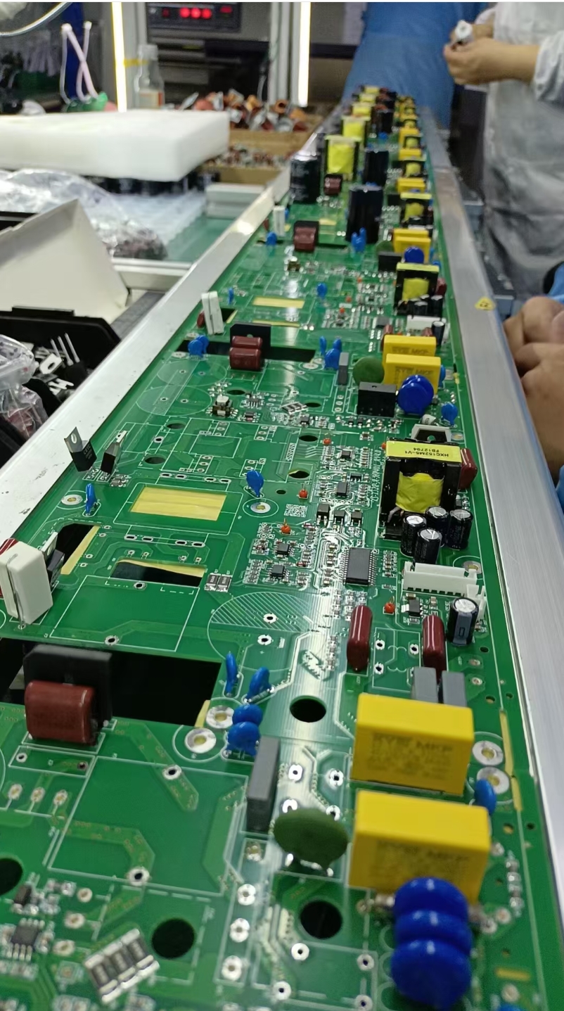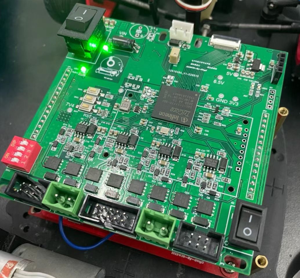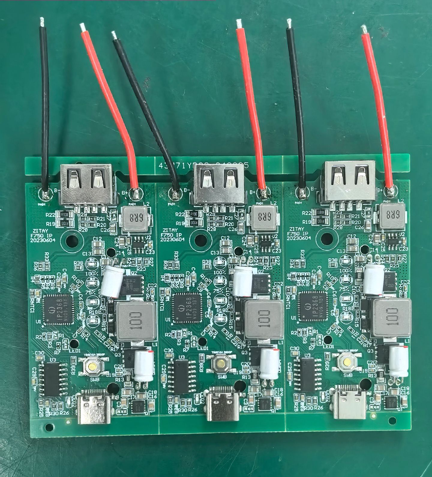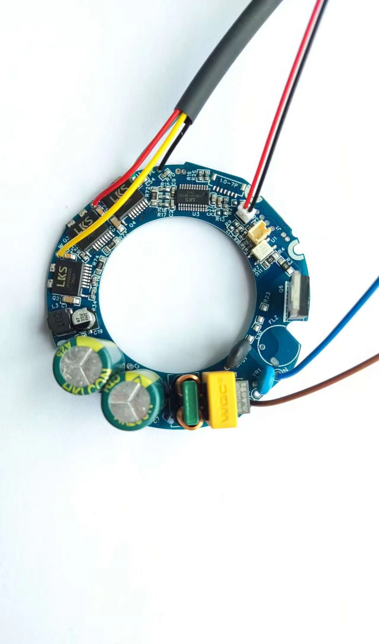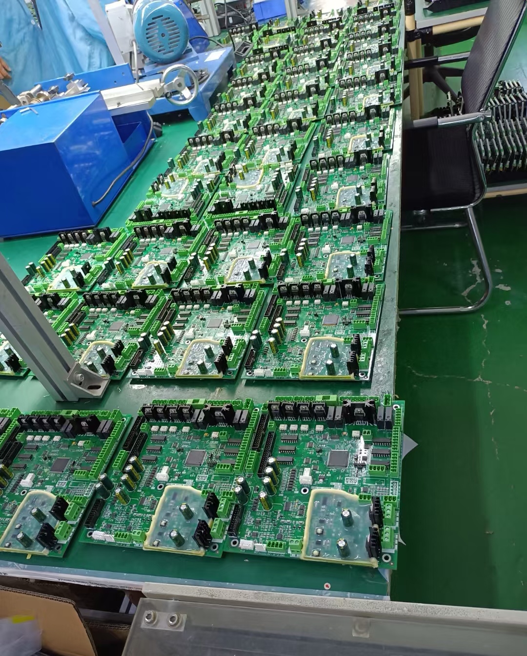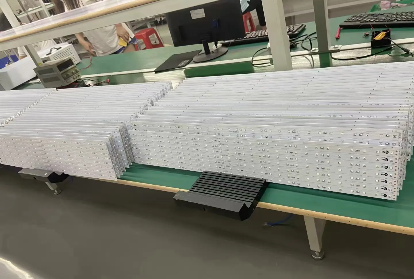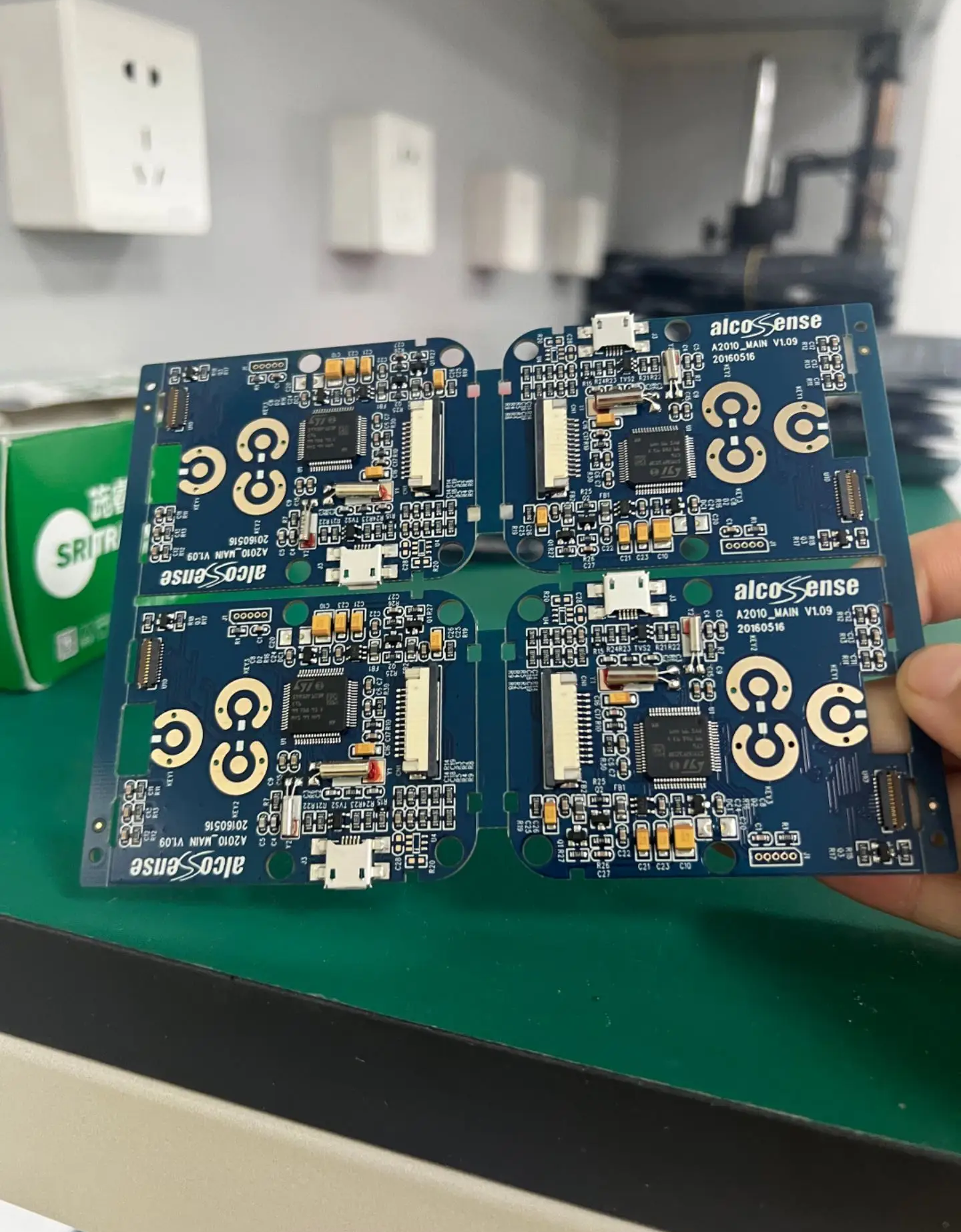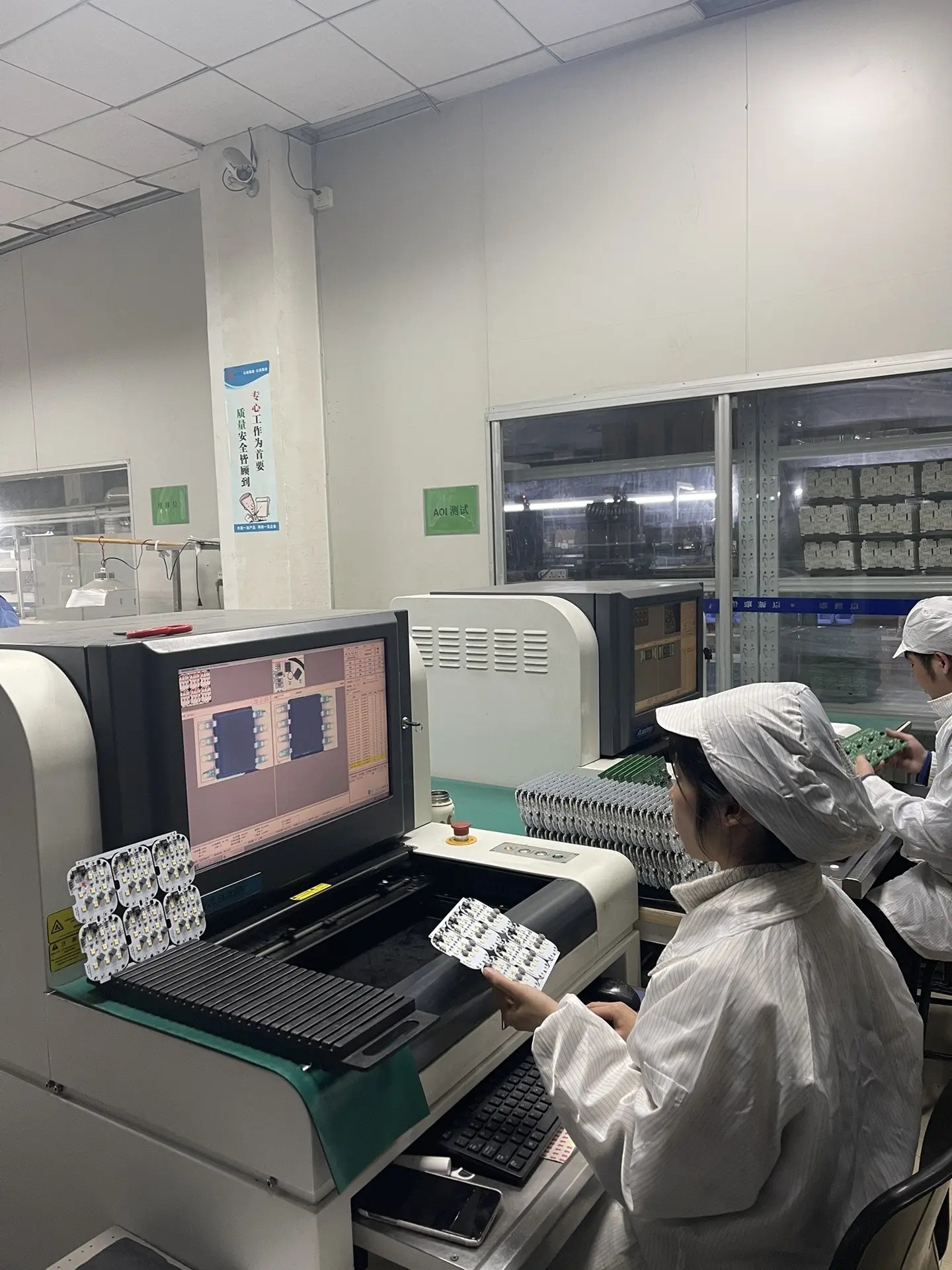
In many PCBs, we can see gold. However, some gold is on the gold fingers, some is used for gold wire bonding, and some is mainly used on the chip's solder pads. You will notice that even though it is all gold, its applications vary greatly. These differences are not just about the thickness of the gold layer, but also involve the composition of the gold, the manufacturing process, and the final application area.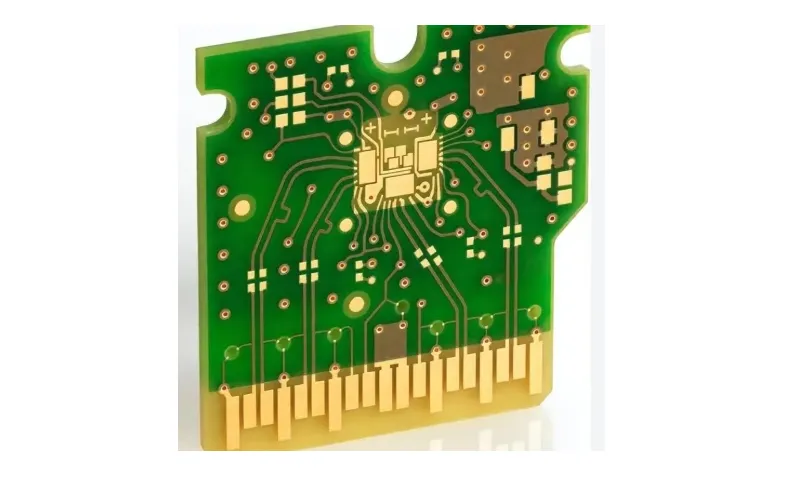
1. Why is some gold wear-resistant, while some is suitable for wire bonding?
Let's first look at two typical applications. For example, the commonly seen gold fingers usually use hard gold. This is easy to understand: gold fingers are frequently inserted and removed. If the wear resistance of the gold layer is poor, it may cause wear and affect contact reliability. Therefore, hard gold is usually applied by electroplating, and the gold layer often contains alloying elements such as cobalt to improve hardness and wear resistance.
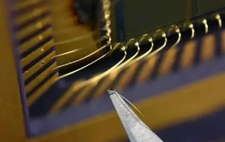
Therefore, the difference between hard gold and soft gold is not simply a matter of thick versus thin, but rather differences in the composition, hardness, and other aspects of the gold layer.
2. Why do PCB solder pads often use Electroless Nickel Immersion Gold (ENIG)?
Electroless Nickel Immersion Gold (ENIG) is a very common surface finish used on many standard PCB solder pads. Its process route involves plating nickel on copper, followed by an immersion reaction to form a thin layer of gold. The fundamental role of this thin gold layer is to protect the underlying nickel. During soldering, the gold will also melt into the solder, ultimately forming a reliable connection through the Tin-Nickel (or Tin-Copper-Nickel) Intermetallic Compound (IMC).
Therefore, the gold layer in ENIG mainly serves to protect the nickel and provide a suitable surface state for subsequent soldering. Unlike the hard gold used for gold fingers, the gold layer in ENIG is usually very thin, with a common thickness of about 0.05~0.1μm.
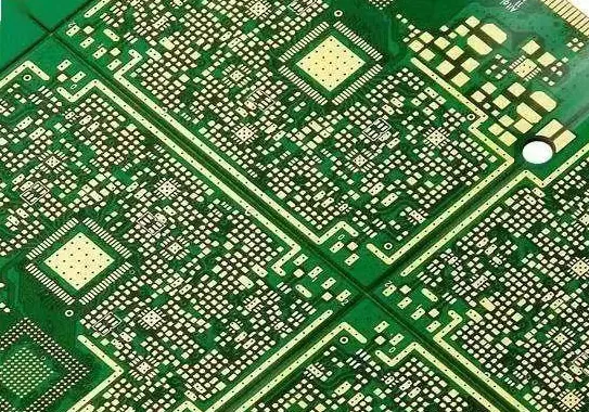
Thus, hard gold, soft gold, and ENIG cannot simply be understood as three different thicknesses of gold. Hard gold and soft gold mainly refer to the composition and performance of the gold layer, whereas ENIG refers to a complete surface finish process.
3. What exactly is Flash Gold?
If the previous types are quite common, then "Flash Gold" is very easy to confuse. Flash Gold is usually associated with thin gold layers, but its usage varies among different documents and suppliers.
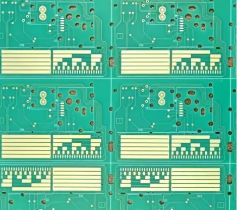
In some contexts, it refers to the thin gold pre-plating layer formed before hard gold electroplating; in other contexts, it is used to describe the thin gold layer on the final product.
Therefore, we cannot simply judge what process is used, how thick the gold layer is, or whether its performance meets the requirements based solely on the name "Flash Gold."
When encountering the term "Flash Gold," further confirmation is needed:
· Process route: Is it a pre-plating before hard gold electroplating, or is it the final surface finish?
· Gold layer thickness: What is the actual thickness, and does it meet the usage requirements?
· Performance requirements: Is it used for contact, soldering, or other purposes? What are the corresponding requirements for wear resistance, solderability, or reliability?
We should note here that a thin gold layer does not necessarily mean poor performance. Whether it ultimately meets the requirements still depends on the specific process, nickel layer condition, gold layer coverage, and operating conditions.
· Hard Gold
Higher hardness, good wear resistance → Gold fingers, connectors.
· Soft Gold
High purity, suitable for specific bonding requirements → Gold wire bonding, etc.
· Electroless Nickel Immersion Gold (ENIG)
Flat surface, relatively thin gold layer → PCB solder pads, fine-pitch components.
· Flash Gold
Usually associated with thin gold layers, specific meaning needs confirmation → Determined based on actual process and application.
Therefore, when it comes to PCB surface finishes, we cannot simply say whether it is gold-plated or not; we must combine it with its actual application:
· Gold fingers: Primarily look at wear resistance.
· Gold wire bonding: Primarily look at bonding compatibility.
· Standard solder pads: Primarily look at solderability and interfacial reliability.
As for Flash Gold, it cannot be judged simply by its name. You must first clarify what specific process it refers to, and then look at the thickness and performance indicators to give it practical meaning.
It's all gold, but different applications require different selection logic.