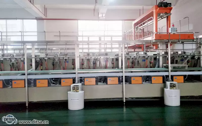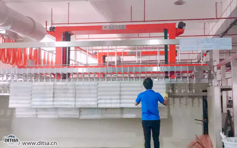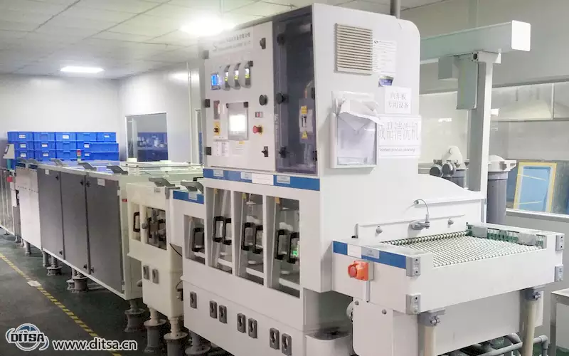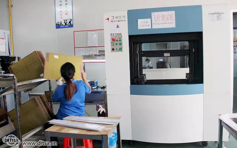
We have our PCB factory in China and PCB-Assembly factory in USA, both of them with fully automated production line to meet what you need. We have our cetifications UL, ISO14001, ISO9001 and TS16949.
DITSA keeps 24 hours respond. We make an response whithin 30 minutes if you need us even in weekends while it's emergency. We provide fast board with 24hours, 48hours and 72hours for 1L-4L PCB and PCBA production.
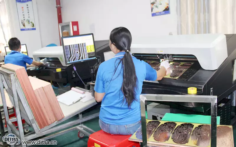
We have our engineers to help to provide you the suggestion on your files or build PCB file, bom list and PCBA file following your requirements. From design your PCB to make the production, we have all-in-one solution.
Quality PCBs. Extraordinary savings. Satisfaction guaranteed.
| Features | Capability | Notes | Patterns |
|---|---|---|---|
| Layer count | 1,2,4,6 layers | The number of copper layers in the board. | |
| Controlled Impedance | 4/6 layer, default layer stack-up | Controlled Impedance PCB Layer Stackup | |
| Material | FR-4 | FR-4 Standard Tg 130-140/ Tg 155 | 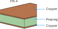 |
| Dielectric constant | 4.5(double-side PCB) |
7628 structure 4.6 2313 structure 4.05 2116 structure 4.25 |
|
| Max. Dimension | 400x500mm | The maximum dimension DITSA can accept | 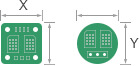 |
| Dimension Tolerance | ±0.2mm | ±0.2mm for CNC routing, and ±0.4mm for V-scoring | |
| Board Thickness | 0.4/0.6/0.8/1.0/1.2/1.6/2.0mm | The thickness of finished board. |  |
|
Thickness Tolerance ( Thickness≥1.0mm) |
± 10% | e.g. For the 1.6mm board thickness, the finished board thickness ranges from 1.44mm(T-1.6×10%) to 1.76mm(T+1.6×10%) | |
|
Thickness Tolerance ( Thickness<1.0mm) |
± 0.1mm | e.g. For the 0.8mm board thickness, the finished board thickness ranges from 0.7mm(T-0.1) to 0.9mm(T+0.1). | |
| Finished Outer Layer Copper | 1 oz/2 oz (35um/70um) | Finished copper weight of outer layer is 1oz or 2oz. | 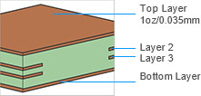 |
| Finished Inner Layer Copper | 0.5 oz (17.5um) | Finished copper weight of inner layer is 0.5oz by default. | 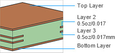 |
| Features | Capability | Notes | Patterns |
|---|---|---|---|
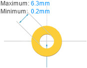
| Drill Hole Size | 0.20mm- 6.30mm0.1mm-0.2mm |
Min. drill size is 0.20mm. Max. drill size is 6.30mm. We have Laser drilling to do 0.1mm-0.2mm holes. |
 |
| Drill Hole Size Tolerance | +0.13/-0.08mm | e.g. for the 0.6mm hole size, the finished hole size between 0.52mm to 0.73mm is acceptable. | |
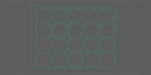
| Blind/Buried Vias | HDI I II III or more | We support all kinds HDI boards and buried vias. | 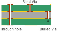 |
| Min. Via hole size | 0.2mm | For Single&Double Layer PCB, the minimum via hole size is 0.3mm;For Multi Layer PCB, the minimum via hole size is 0.2mm | 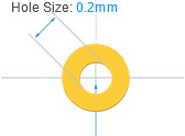 |
| Min. Via diameter | 0.4mm | For Single&Double Layer PCB, the minimum Via diameter is 0.6mm;For Multi Layer PCB, the minimum via diameter is 0.4mm. | 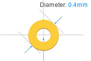 |
| PTH hole Size | 0.20mm - 6.35mm | The annular ring size will be enlarged to 0.15mm in production. | 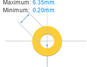 |
| Pad Size | 0.70mm- 6.35mm | The pad hole size will be enlarged 0.15mm in production. | 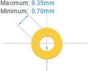 |
| Min. Non-plated holes | 0.50mm | The minimum NPTH dimension is 0.50mm, Please add the NPTH in the mechanical layer or keep out layer. | 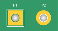 |
| Min. Plated Slots | 0.65mm | The minimum plated slot width is 0.65mm, which is drawn with a pad. | 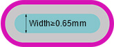 |
| Min. Non-Plated Slots | 1.0mm | The minimum Non-Plated Slot Width is 1.0mm, please draw the slot outline in the mechanical layer(GML or GKO) | 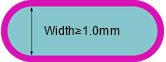 |
| Min. Castellated Holes | 0.60mm | The minimum diameter of castellated holes is 0.60mm. | 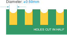 |
| Hole size Tolerance (Plated) | +0.13mm/-0.08mm | e.g. for the 1.00mm Plated hole, the finished hole size between 0.92mm to 1.13mm is acceptable. | 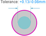 |
| Hole size Tolerance (Non-Plated) | ±0.2mm | e.g. for the 1.00mm Non-Plated hole, the finished hole size between 0.80mm to 1.20mm is acceptable. | 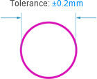 |
| Rectangle Hole/Slot | Yes |  |
| Minimum annular ring | PTH | Patterns | |
|---|---|---|---|
| 1oz Copper | 0.13mm | 0.3mm | 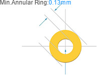 |
| 2oz Copper | 0.2mm | 0.3mm |
| Features | Capabilities | Patterns |
|---|---|---|
| Hole to hole clearance(Different nets) | 0.5mm |  |
| Via to Via clearance(Same nets) | 0.254mm | |
| Pad to Pad clearance(Pad without hole, Different nets) | 0.127mm | 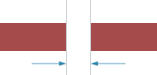 |
| Pad to Pad clearance(Pad with hole, Different nets) | 0.5mm | |
| Via to Track | 0.254mm |  |
| PTH to Track | 0.33mm | |
| NPTH to Track | 0.254mm | |
| Pad to Track | 0.2mm | |
| Copper weight | Min. Trace width | Min. Spacing | Patterns |
|---|---|---|---|
| H/HOZ (Inner layer) | 5mil (0.127mm) | 5mil (0.127mm) | 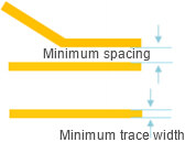 |
| 1oz (Outer layer) | 1/2 layers: 5mil (0.127mm) 4/6 layers: 3.5mil(0.09mm) |
1/2 layers: 5mil (0.127mm) 4/6 layers: 3.5mil(0.09mm) |
|
| 2oz (Outer layer) | 8mil (0.2mm) | 8mil (0.2mm) |
| Layer count | Min. BGA Pad Dimensions | Min. Distance Between BGA | Patterns |
|---|---|---|---|
| 1/2 layers | 0.4 mm | 0.127mm | 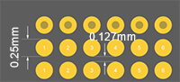 |
| 4/6 layers | 0.25 mm | 0.127mm |
| Features | Capabilities | Notes | Patterns |
|---|---|---|---|
| Solder mask opening/ expansion | 0.05mm | The solder mask should have a minimum of a 0.05 mm "growth/mask opening" around the pad to allow for any mis-registration. | 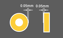 |
| Solder bridge |
0.2mm(green) 0.254mm(other colors) |
To have solder mask bridge, the spacing between copper pads edge must be 0.2mm (8mils) or more. | 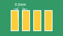 |
| Solder mask color | green, red, yellow, blue, white, black, grey or any colors. | We can make any colors you request by fixing. | |
| Solder mask dielectric constant | 3.8 | ||
| Solder mask thickness | 10-15UM |
| Features | Capabilities | Notes | Patterns |
|---|---|---|---|
| Minimum Line Width | 6 mil (0.153mm) | Characters width less than 6mil(0.153mm) will be unidentifiable. | 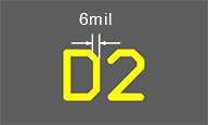 |
| Minimum text height | 32 mil (0.8mm) | Characters height less than 32mil(0.8mm) will be unidentifiable. |  |
| Character width to height ratio | 1:6 | The preferred ratio of width to height is 1:6. | 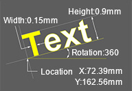 |
| Pad To Silkscreen | 0.15mm | The Minimum Distance Between Pad and Silkscreen is 0.15mm. | 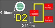 |
| Features | Capabilities | Notes | Patterns |
|---|---|---|---|
| Trace to Outline | 0.2mm | Ships as individual board(Rounting):Trace to Outline≥0.2mm | 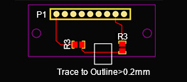 |
| Trace to V-cut line | 0.4mm | Ship as panel with V-scoring: Trace to V-cut line≥0.4mm | 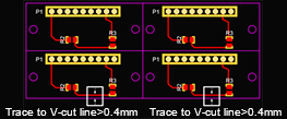 |
| Features | Capabilities | Notes | Patterns |
|---|---|---|---|
| Panelization without space | 0mm | The space between boards is 0mm. | 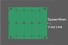 |
| Panelization with space | 2mm | Make sure the space between boards should be ≥2mm,otherwise it will be hard to process for rounding. | 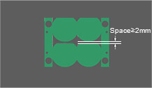 |
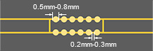
| Panelized Round board | ≥20mmx20mm |
The single round board size should be≥20mmx20mm. Panelize with stamp holes and add tooling strips on four board edges |
 |
| Panelized castellated holes board | Panelize with stamp holes and add tooling strips on four board edges |
The distance between castellated hole and board corner should be larger than 4mm. Recommended diameter of stamp hole is 0.5mm-0.8mm; Recommended distance between the two stamp holes is 0.2-0.3mm |
|
| Min. Width of Breakaway Tab | 4mm | The minimum width of breakaway tab is 4mm. For breakaway with mouse-bites, the minimum width is 5mm. | 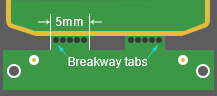 |
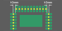
| Min. Edge Rails | 3mm | If choosing panel by DITSA, we will add 5mm edge rails on both sides by default. | 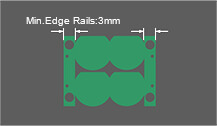 |