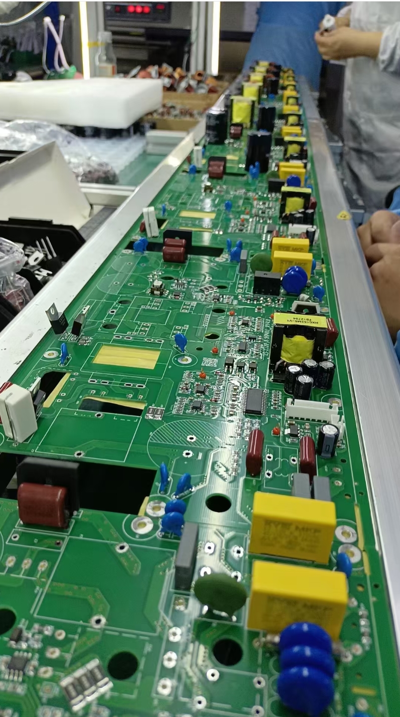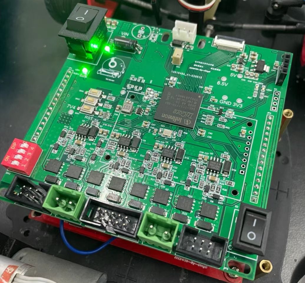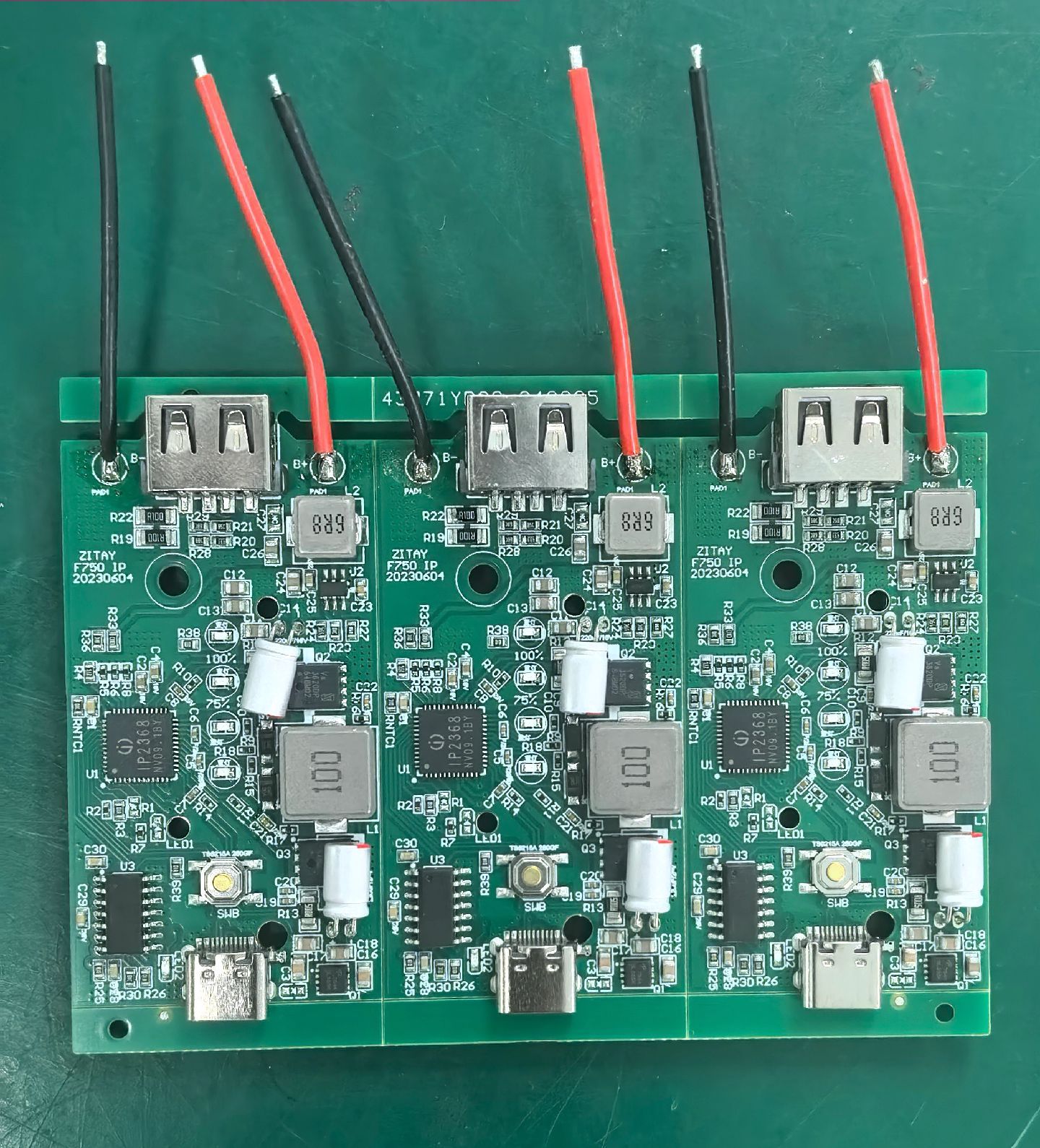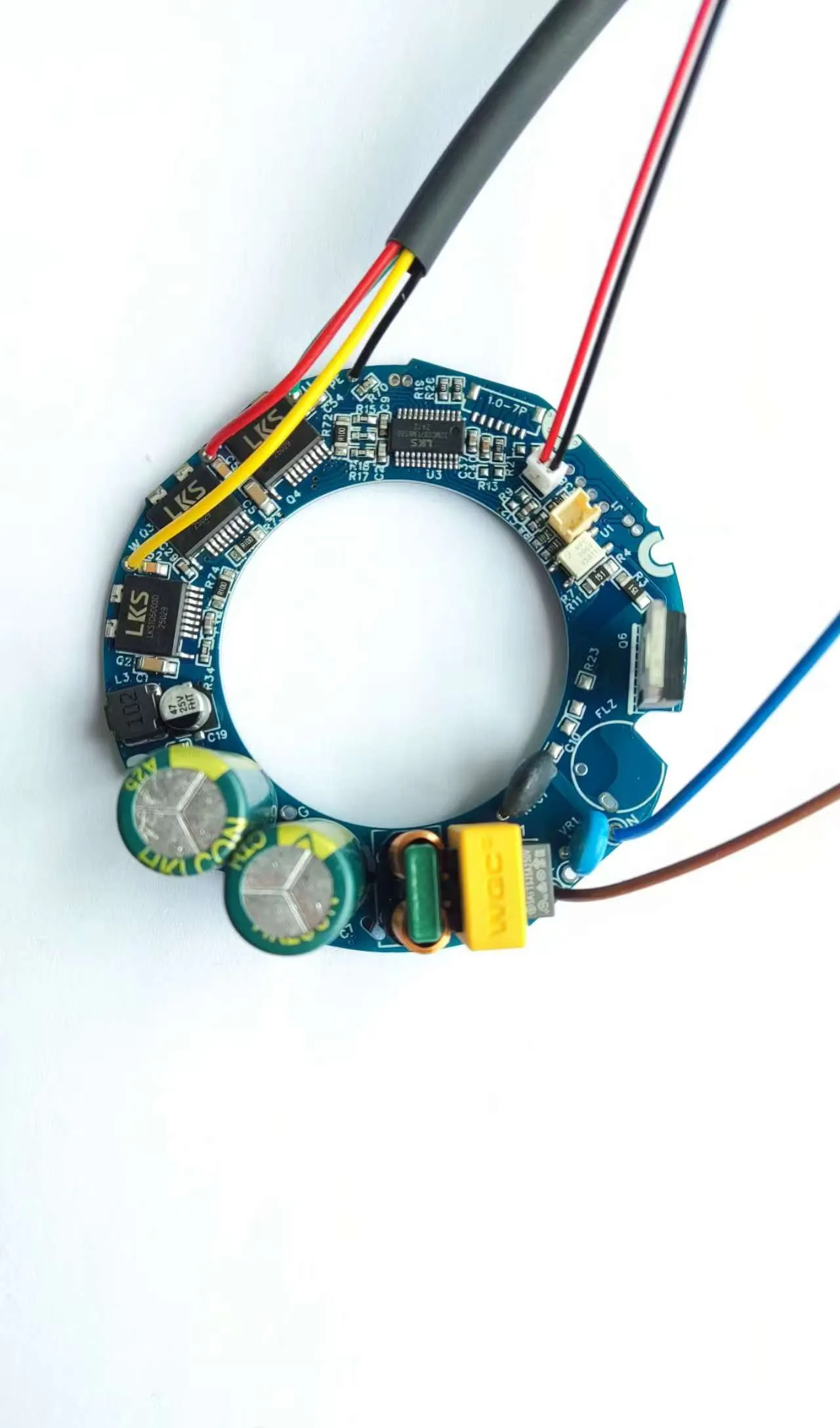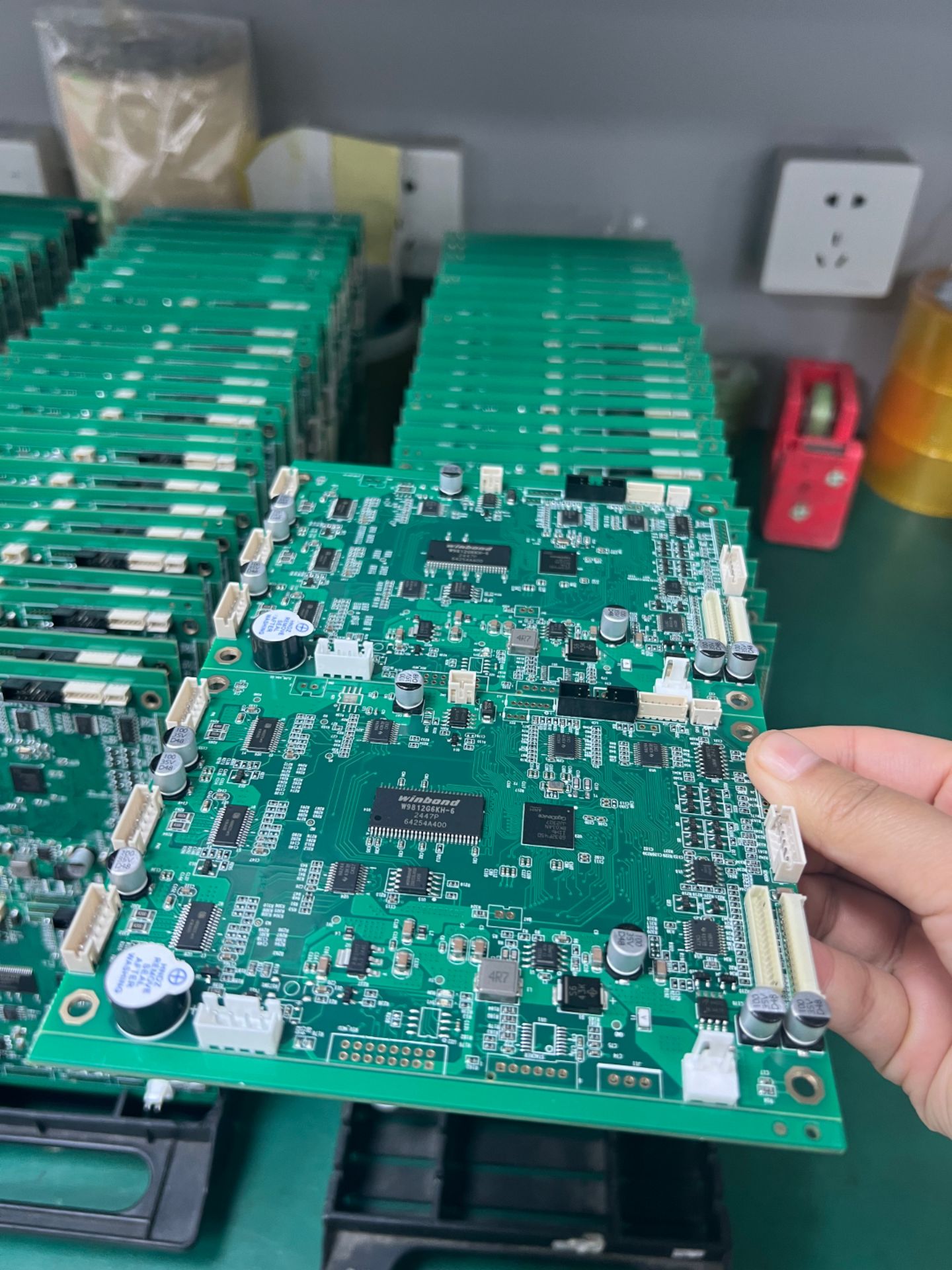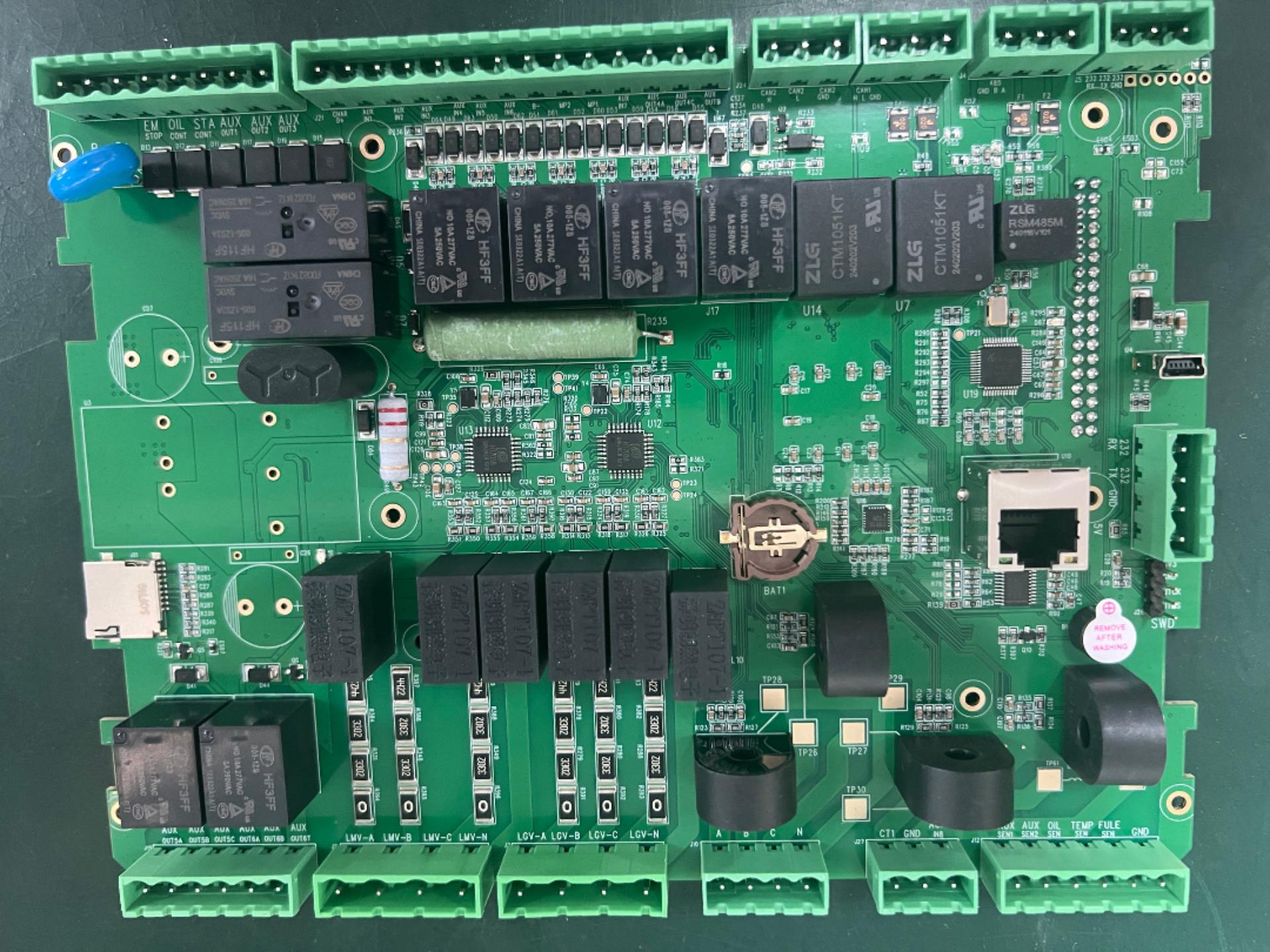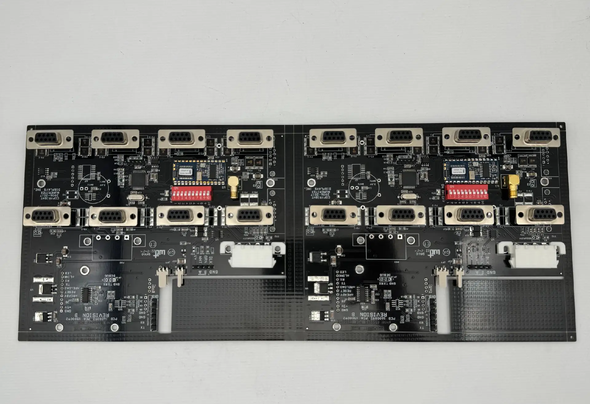
I often see Gerbers where traces run very close to the board outline, or pads are placed right at the edge. Customers think this saves space.
But from a PCB manufacturing and processing perspective, the board edge is not waste — it is a production interface.
If the board edge is designed casually, these problems can easily appear later:
1. Routing and depaneling can damage traces, cause edge chipping, or expose copper
Routing tools have cutting paths and tolerances, and V-CUT also has depth and clearance requirements. If traces, pads, or copper foil are too close to the outline, stress during depaneling can transfer to the board edge, causing chipping, burrs, exposed copper, or even damage to circuits.
2. SMT and reflow require conveyor edges and clamping edges
If the board edge has cutouts, components are too close to the edge, or there is no process edge, pick-and-place machines may have unstable clamping and conveying, and reflow/wave soldering may also be affected. Saving a little board edge can lead to line stops, misalignment, and lower yield.
3. Panelization and fiducial marks need space
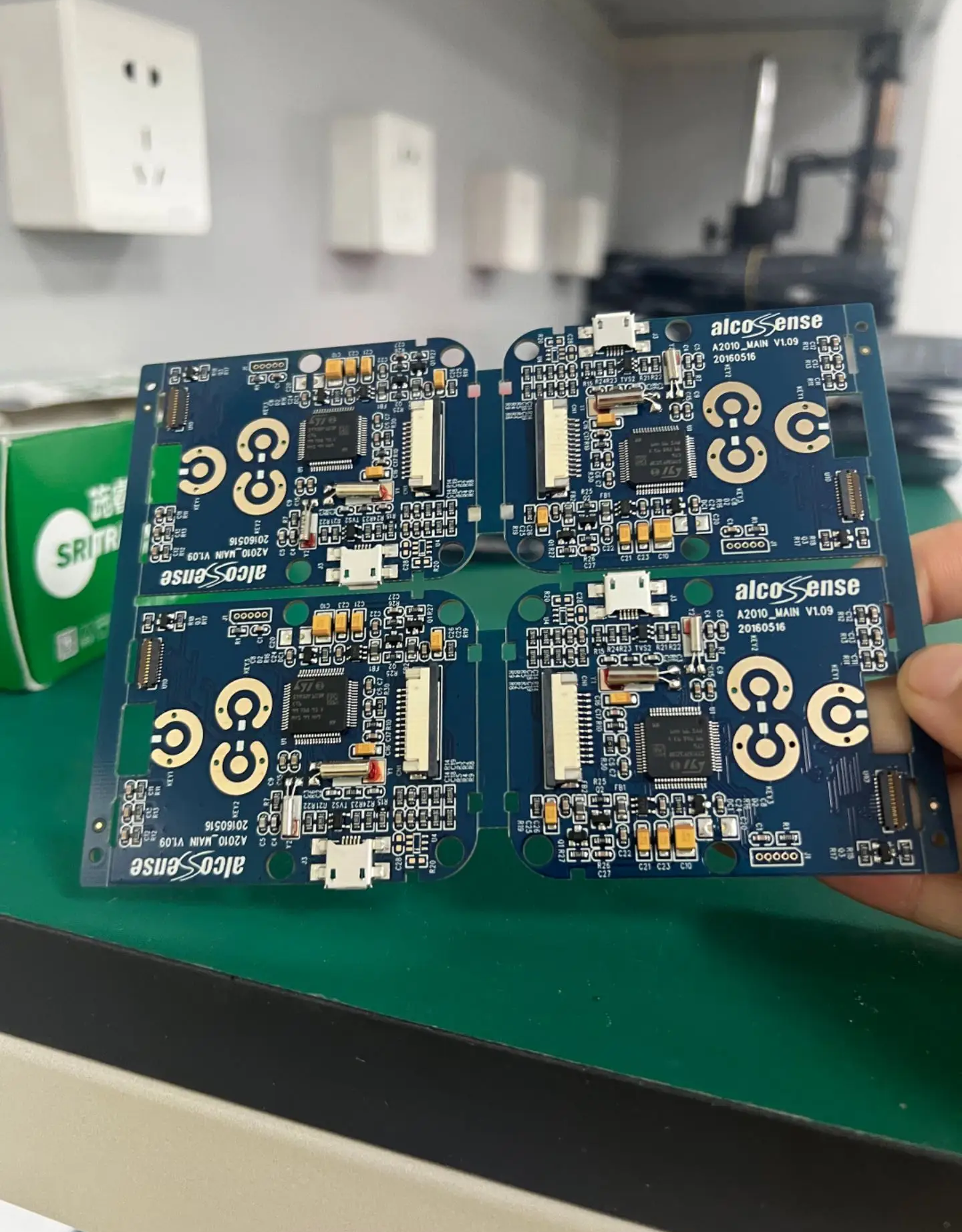
The process edge is not “wasted area.” It needs to provide space for equipment clamping, fiducial marks, tooling holes, test points, and V-CUT connecting webs. If the panelization method is not confirmed and the board edge is slotted casually, both production and depaneling will become difficult.
4. Copper and solder-mask openings too close to the edge can cause appearance and safety issues
Large copper areas, exposed copper, or solder-mask openings too close to the outline can lead to oxidation, burrs, exposed copper, and in some products, creepage distance and safety requirements must also be considered.
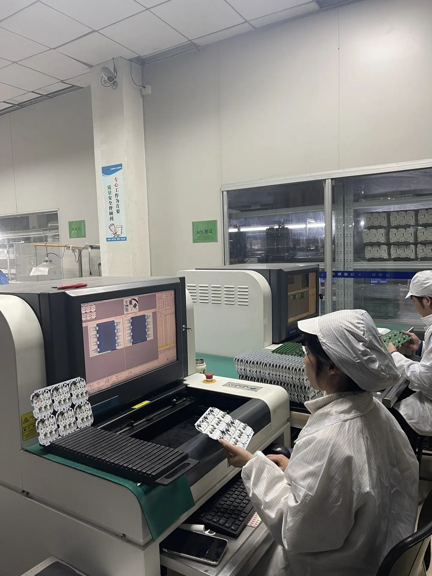
5. AOI, test fixtures, and depaneling fixtures need clearance and positioning
Board edge design is not only about “whether it can be made,” but also about whether inspection, testing, and depaneling can run smoothly afterward. If fixture clearance is insufficient, the production team will have to adjust repeatedly.
So for board edge design, I usually recommend customers confirm three things first:
① Keep a safe distance between critical traces, pads, and copper foil and the board outline;
② Confirm whether panelization, SMT, V-CUT, or stamp holes are needed;
③ Confirm how to reserve process edges, fiducial marks, and tooling holes.
Specific values depend on each factory’s equipment capability and are subject to engineering review, but the principle is: the board edge must leave space for routing, depaneling stress, equipment clamping, and inspection.
In one sentence: the board edge is not just “draw it up to the outline.” It is a production interface. The few millimeters saved on board edge design may come back in yield, lead time, and customer complaints.