
PCBA refers to the complete process of assembling electronic components onto bare PCB boards, including core steps: preliminary preparation, SMT mounting, DIP through-hole assembly, post-soldering cleaning, routine testing, program burning, aging test, final inspection and warehousing. It is suitable for actual factory production while balancing efficiency and quality.
I. Preliminary Preparation Stage
1. Engineering Document Review
Receive customers' Gerber files, BOM lists, coordinate files and assembly drawings, conduct DFM analysis for manufacturability, identify potential production risks and confirm production plans.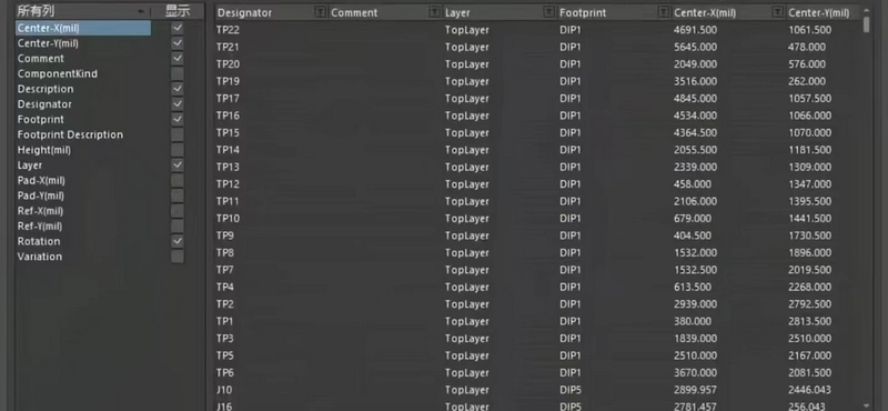
2. Incoming Material Inspection
Inspect bare PCB boards for appearance, dimensions, scratches, deformation, open or short circuits. Verify electronic components for correct model and appearance to prevent defective or wrong materials from entering the production line.
3. Auxiliary Materials & Equipment Calibration
Prepare solder paste, flux, stencils, fixtures and other auxiliary materials. Calibrate printers, mounters, reflow ovens, wave soldering machines and other equipment to ensure stable operation.
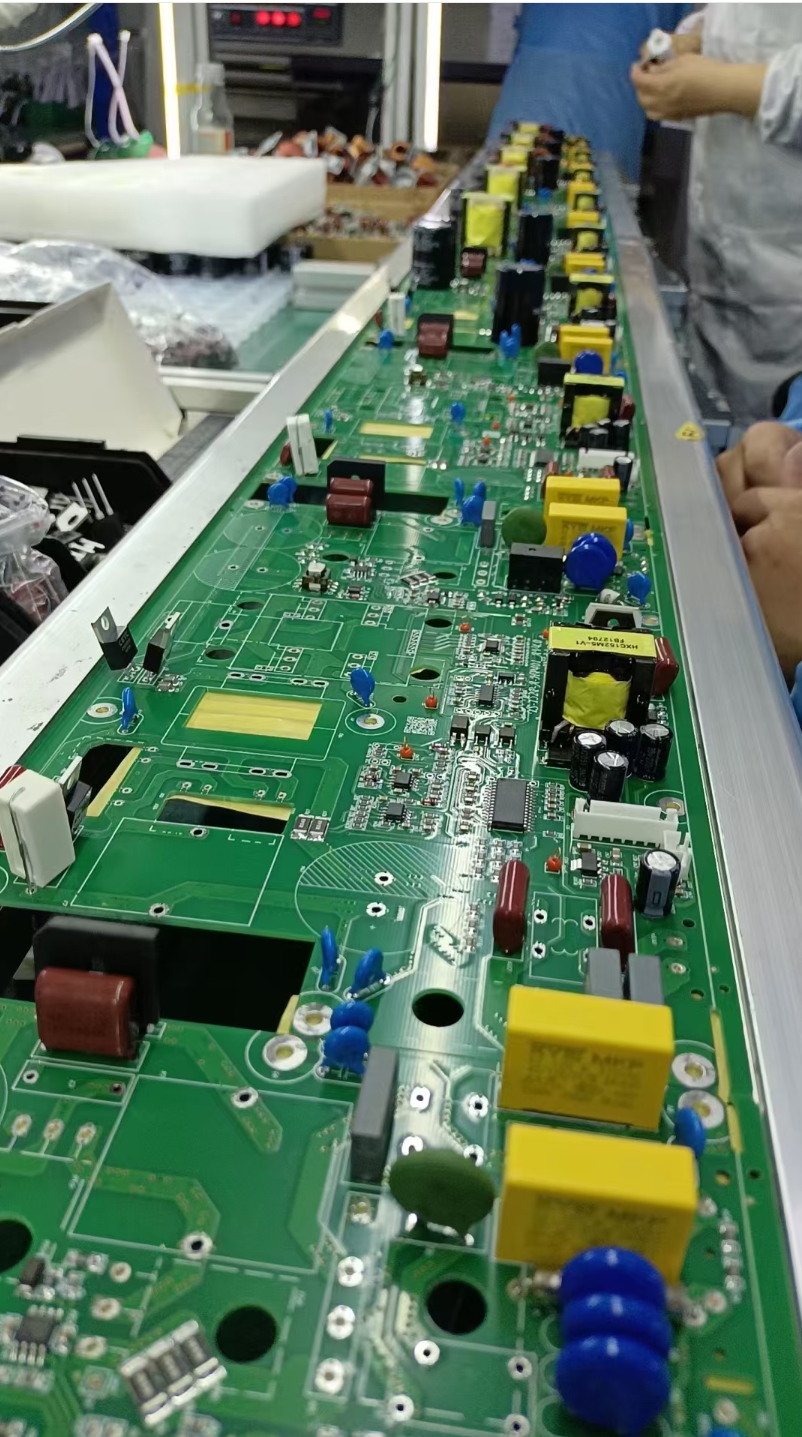
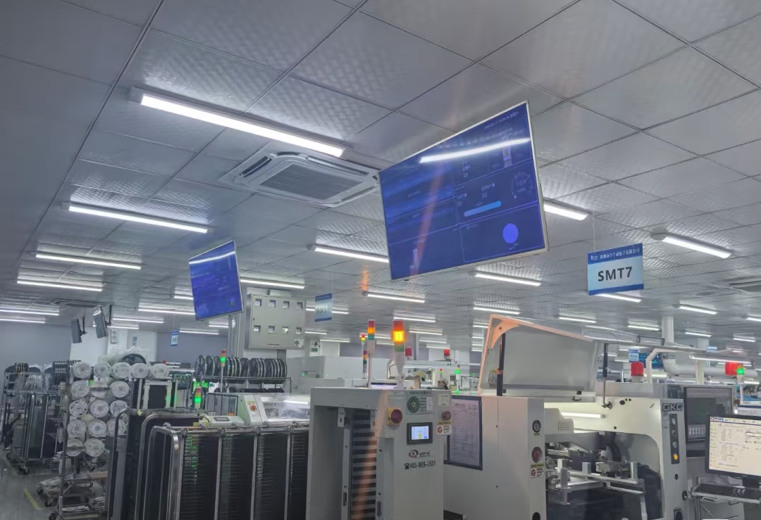
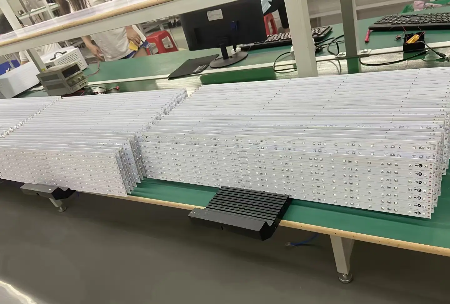
II. SMT Surface Mount Process
1. Solder Paste Printing
Use an automatic solder paste printer to evenly apply solder paste on PCB pads. Control printing accuracy to avoid insufficient solder, missing printing or offset, and conduct first-article verification.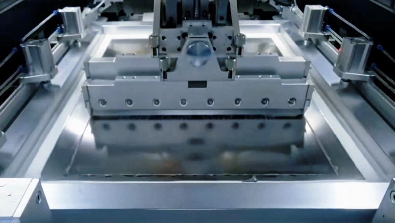
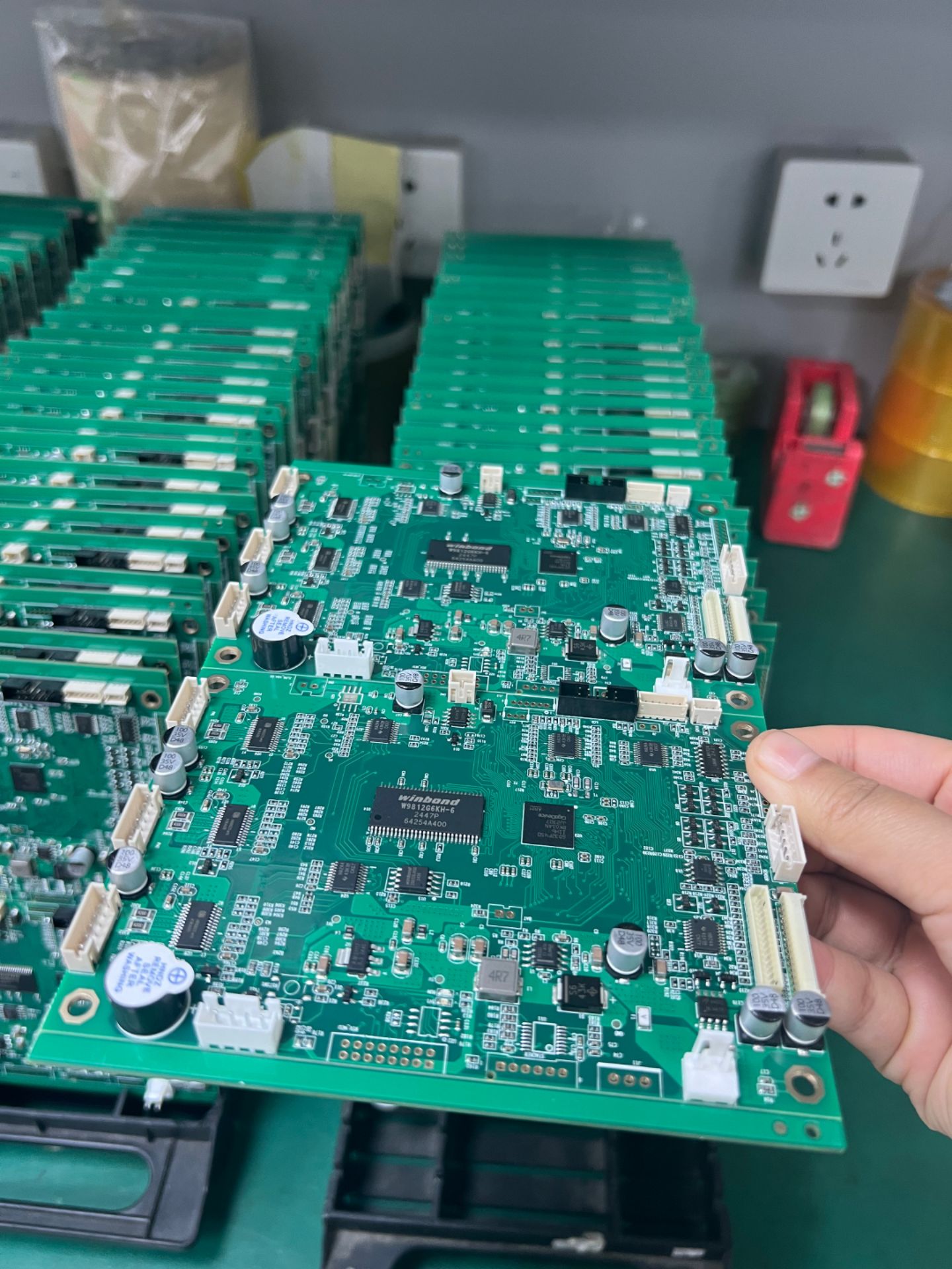
2. Component Placement
Mount SMD components accurately to designated positions via high-speed placement machines, strictly controlling placement deviation to ensure proper positioning.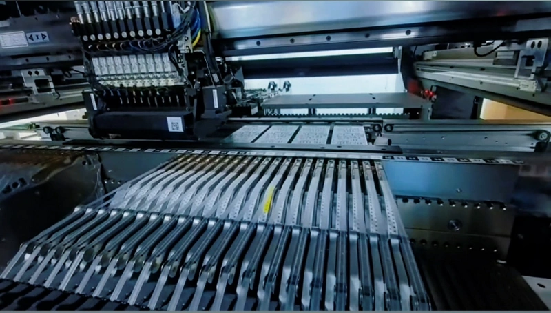
3. Reflow Soldering
Feed PCBs into a reflow oven to complete preheating, soldering and cooling according to set temperature profiles, allowing solder paste to solidify into firm solder joints and avoid cold joints or false soldering.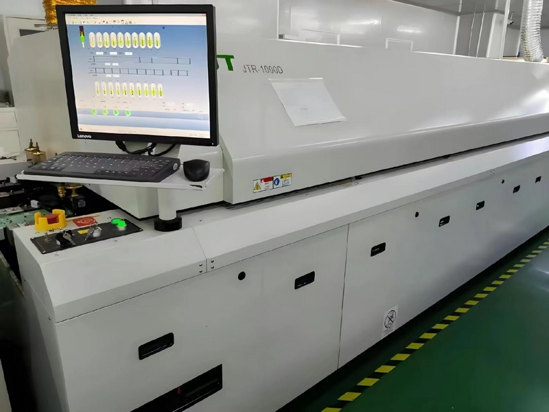
4. SMT First-Article Inspection
Inspect the first article before mass production to verify components, solder joints and placement. Mass production starts only after approval.
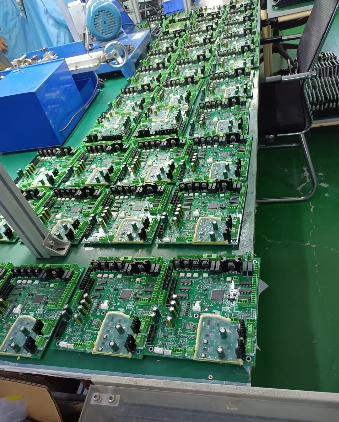
III. DIP Through-Hole Assembly Process
1. Manual Insertion
Insert through-hole components such as high-power capacitors, inductors and connectors into corresponding PCB holes, ensuring correct polarity without mis-insertion or omission.
2. Wave Soldering
Solder inserted PCBs via wave soldering and automatically cut excess pins. Manual touch-up soldering is applied at precise positions to ensure reliable joints.
IV. Post Processing
1. Solder Joint Repair
Trim excess pins and manually repair defective joints such as cold joints, bridging or insufficient solder, with re-inspection after repair.
2. Cleaning
Use environmental cleaning solvent or ultrasonic cleaning to remove flux residue, solder balls and dust to prevent short circuits.
V. Routine Testing
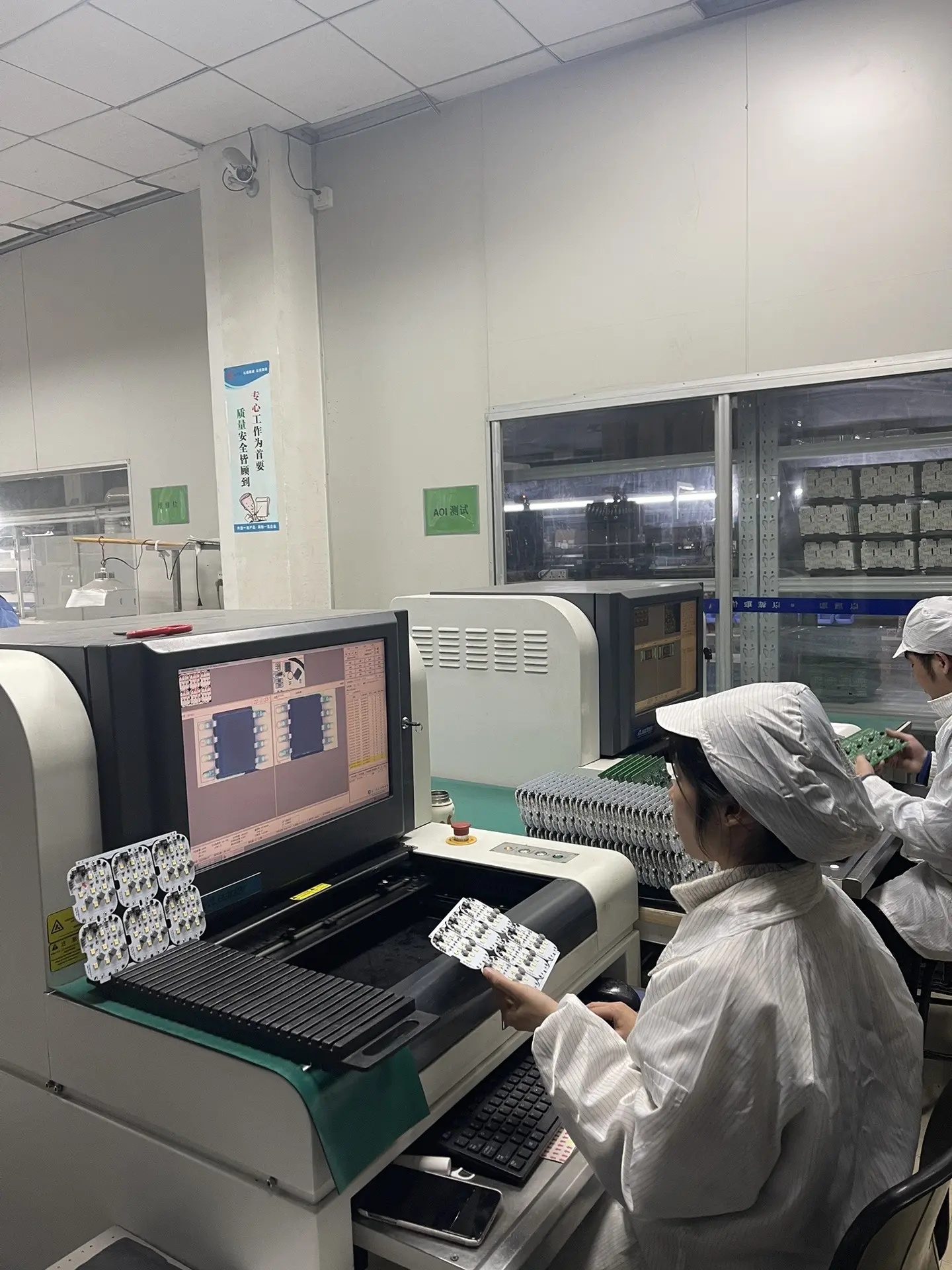
1. AOI Visual Inspection
Scan and inspect component placement and solder joint appearance via automatic optical inspection (AOI) to filter defects such as wrong components, cold joints or bridging.
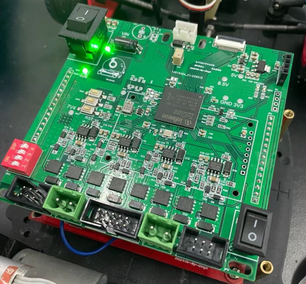
2. Basic Functional Test
Power on and test basic functions of PCBs to verify normal operation and eliminate defective units.
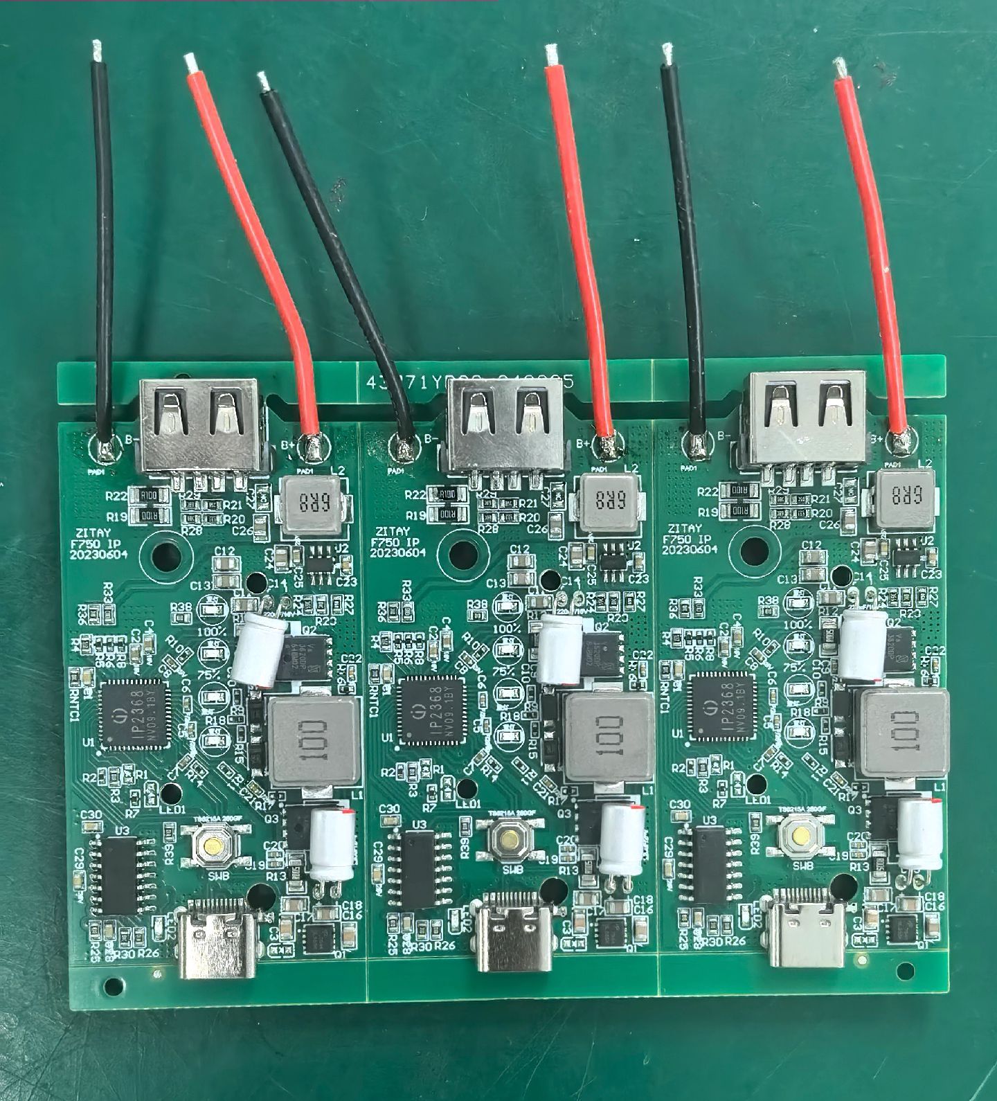
Final Inspection & Warehousing
1. Final Inspection
Comprehensively check appearance and functions to ensure no defects.
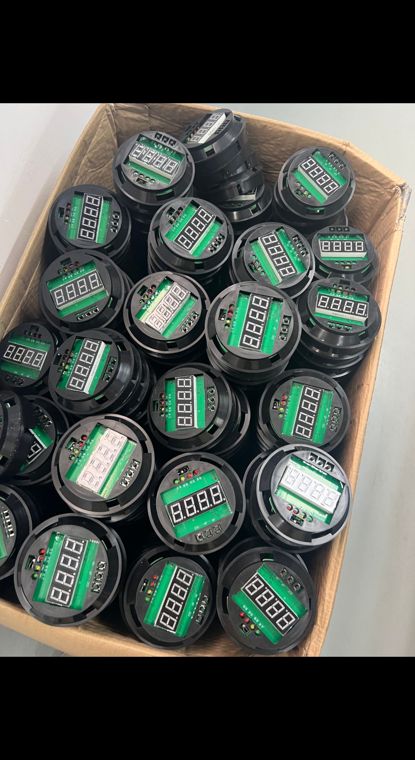
2. ESD Packaging & Warehousing
Package with ESD bags and foam to prevent electrostatic damage and bumps. Qualified products are stored for delivery.
Full-Process Quality Control
Implement incoming material inspection, in-process patrol inspection and finished product sampling inspection to control quality throughout the process, avoid mass defects and ensure qualified delivery.


10585 View