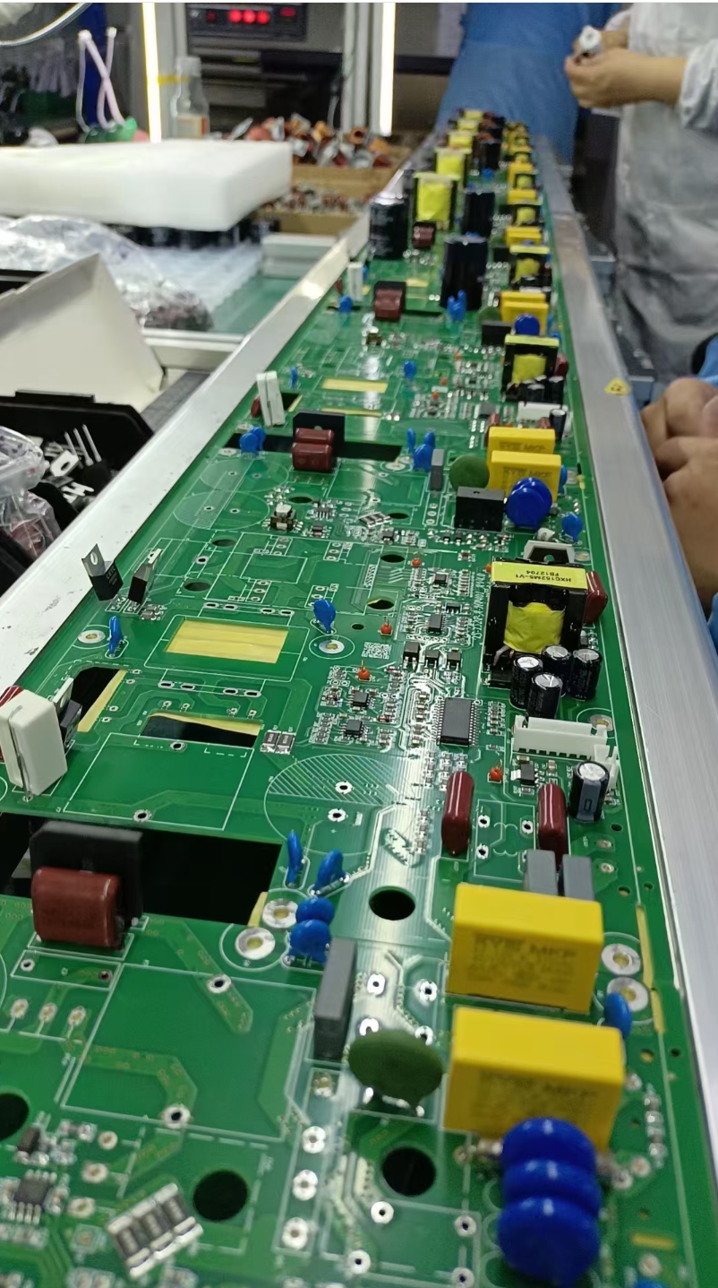
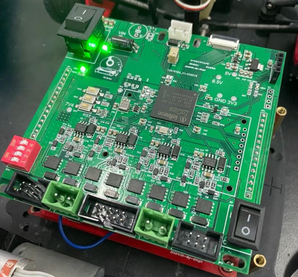
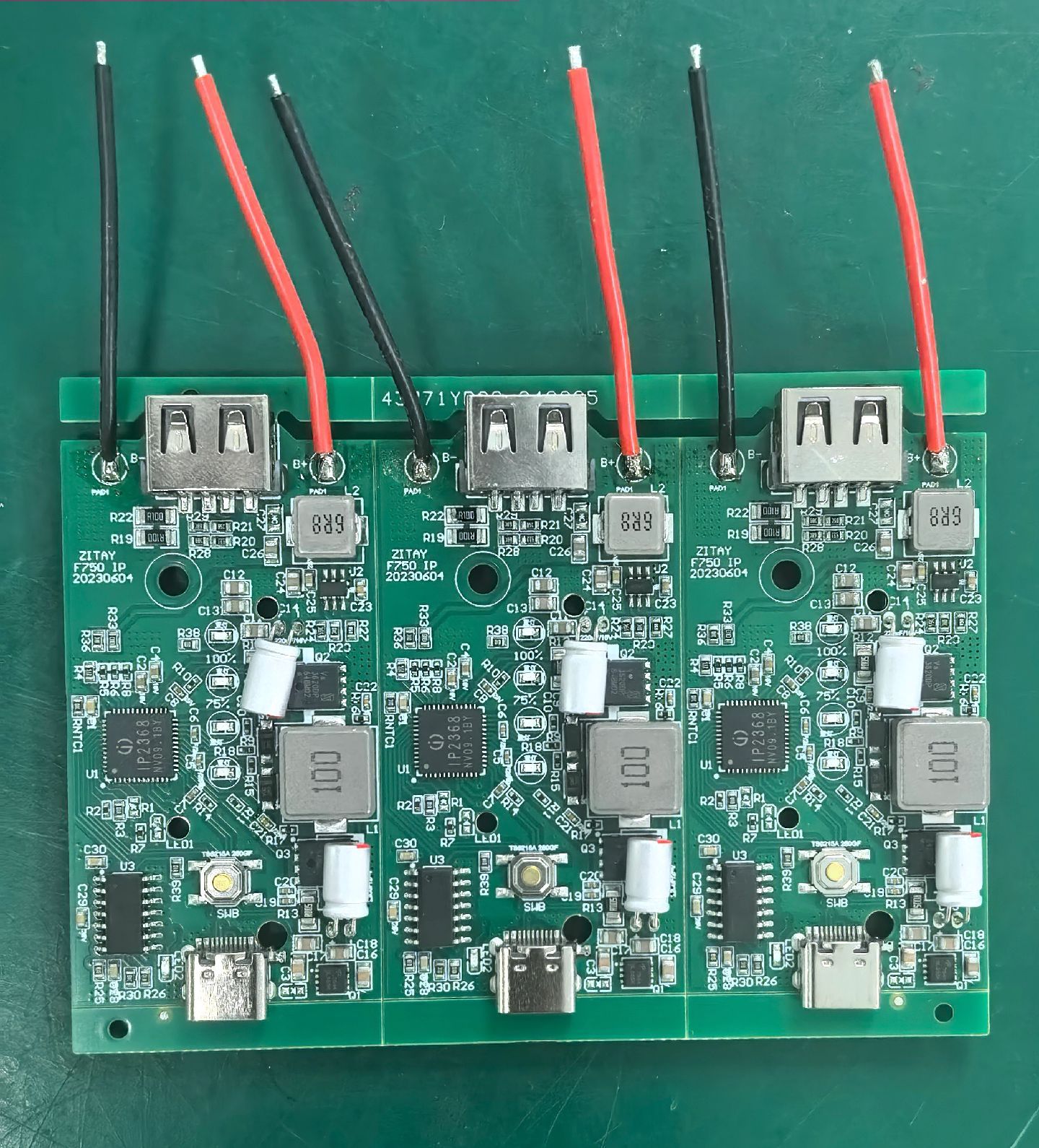
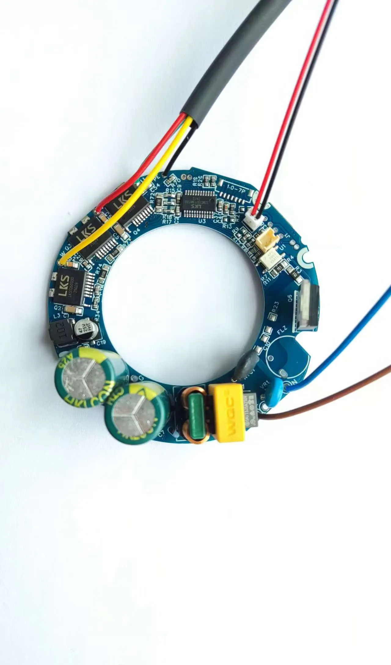
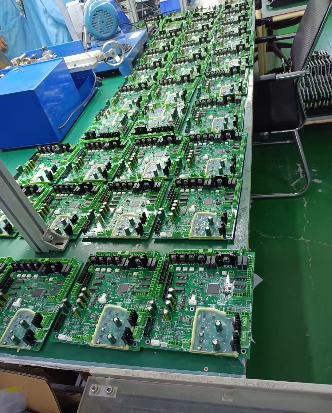
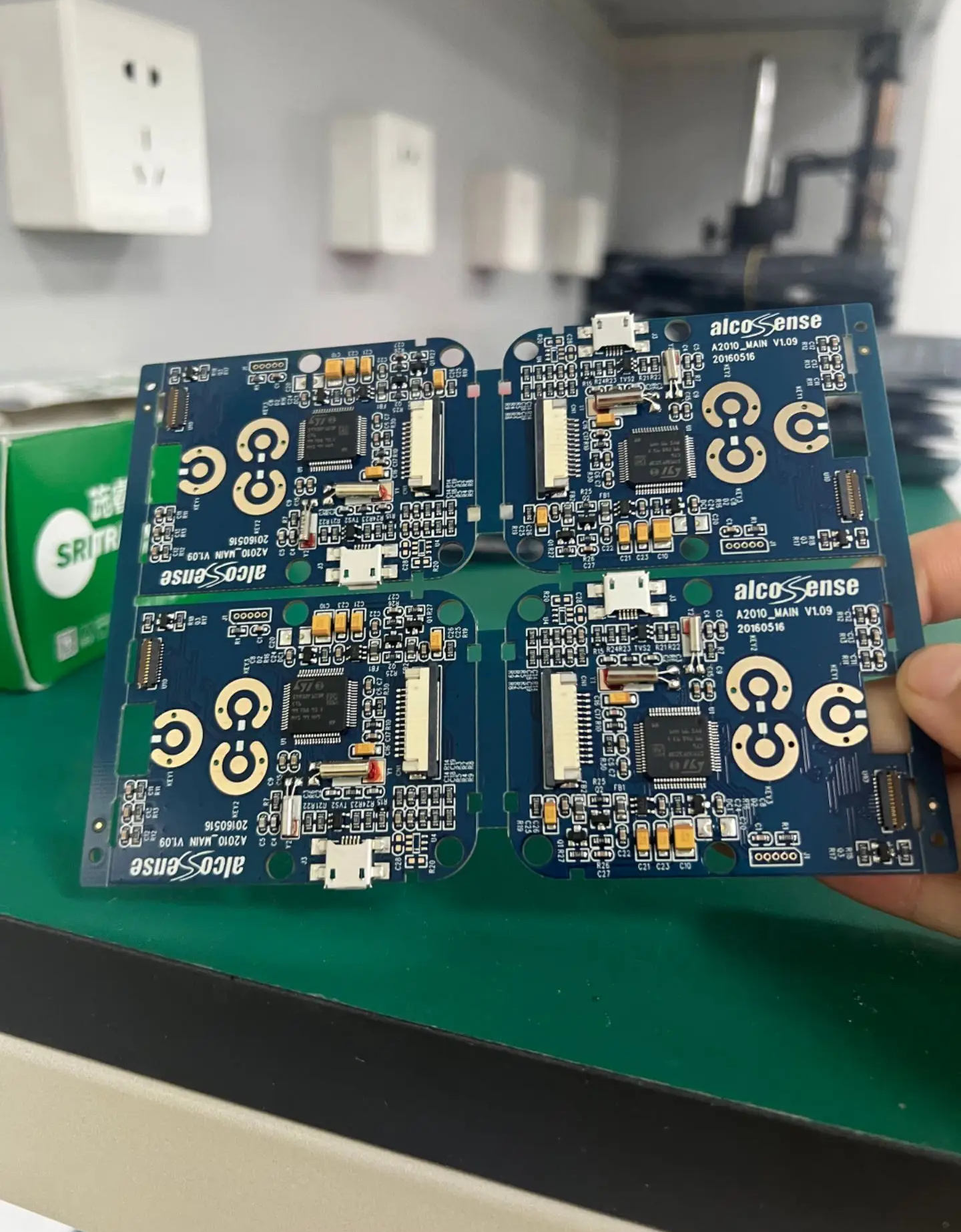
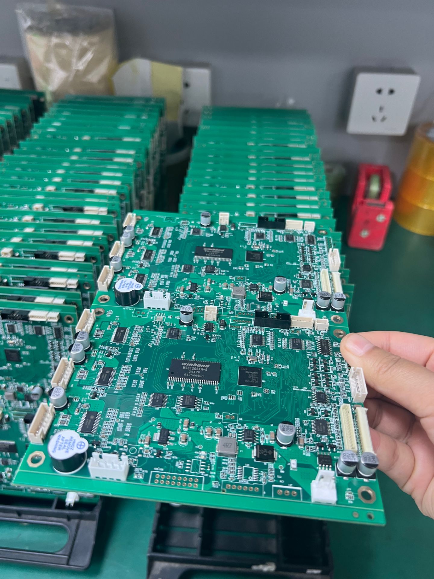
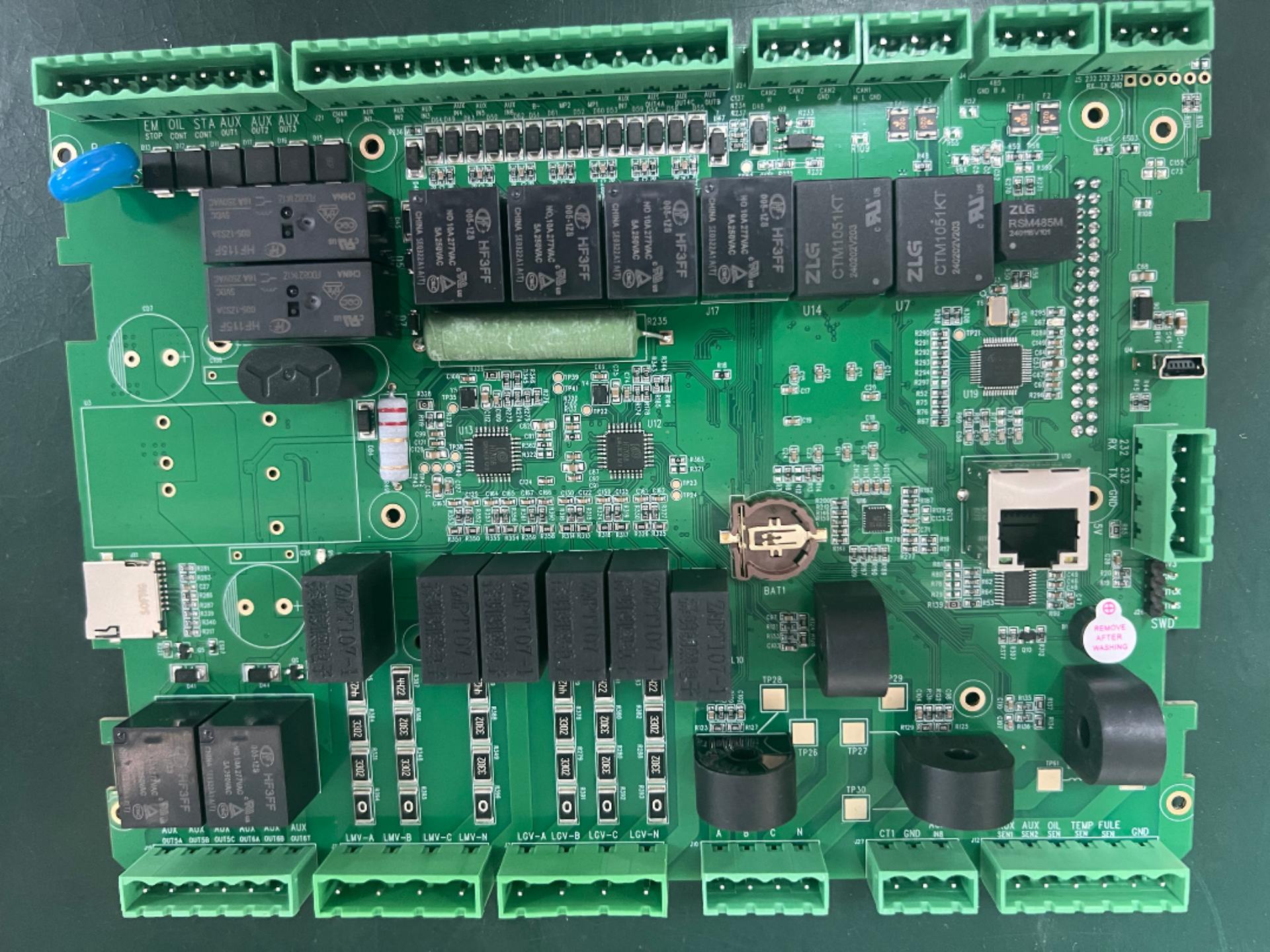
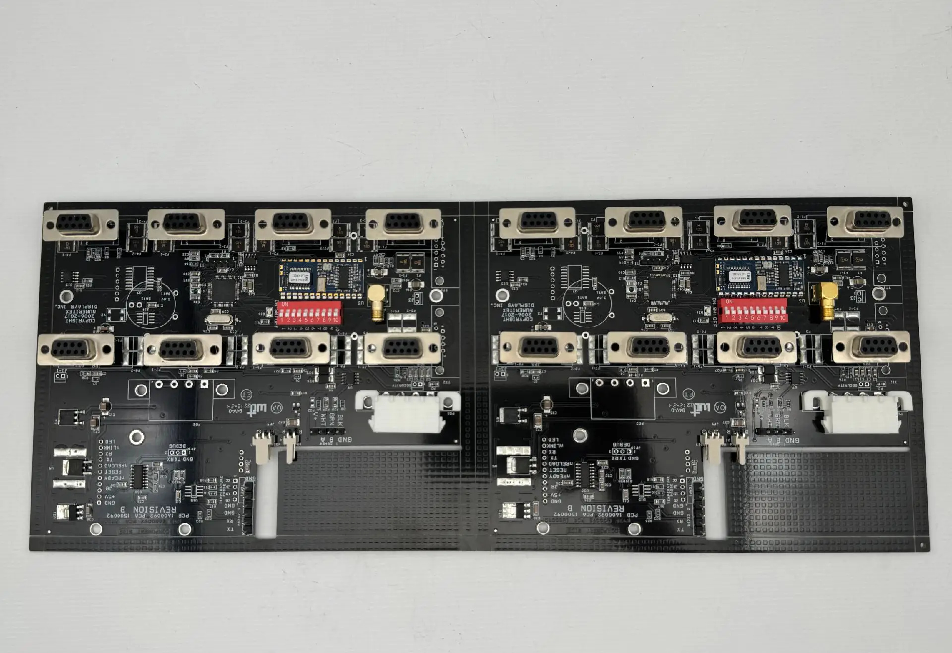
Why can't the crystal oscillator be placed on the edge of the PCB? Take a practical example: There is a board with a 12MHz crystal placed on the edge of the PCB, and as a result, the radiation exceeds the standard during the power-on test! The reason is that when the product is in the radiation test environment, a parasitic capacitance will be formed between the high-speed device and the reference ground.
If the crystal oscillator is too close to the edge of the PCB, it will cause the electric field to be distributed to the external reference ground and the common-mode radiation will become stronger. However, if the crystal oscillator is placed in the middle of the PCB, the ground plane can enclose the electric field and most of the energy is shielded inside the board, so the radiation is significantly reduced. Remember, don't place the crystal oscillator on the edge, place it in the middle of the board, and the radiation will naturally be reduced by half!
10393 View

