
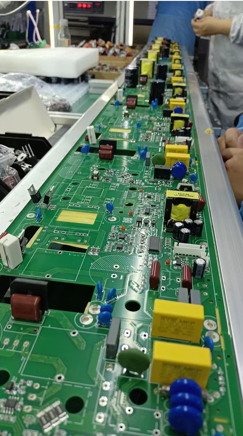
1. Pitfall: Mismatched Pad and Component Pin Sizes
- Common Mistake: Pad dimensions are more than 20% larger or smaller than component pins
- Consequence: Cold solder joints, short circuits, or component placement offset
- Correct Practice: Refer to the pad footprint library provided in the component datasheet and prioritize using standard footprints supplied by the manufacturer
2. Pitfall: Insufficient Distance Between Vias and Conductors
- Common Mistake: Distance from via edge to conductor is less than 0.2mm
- Consequence: High risk of short circuits during production and difficulty in post-maintenance
- Correct Practice: Maintain a distance of ≥0.3mm (can be relaxed to 0.2mm for high-density boards, but must confirm process capability with the manufacturer in advance)
3. Pitfall: Unoptimized Copper Pour
- Common Mistake: Large-area copper pour without grid pattern or unconnected to GND
- Consequence: Thermal deformation, signal interference, or uneven electroplating
- Correct Practice: Use grid-style copper pour for large areas and connect to the nearest GND network
4. Pitfall: No Allowance for Mounting/Hole Positions
- Common Mistake: Mounting hole size exactly matches the screw size
- Consequence: Assembly failure due to hole position deviation
- Correct Practice: Make mounting hole diameter 0.2-0.5mm larger than the screw (e.g., 3.2-3.5mm hole for M3 screws)
5. Pitfall: Mismatched Conductor Width with Current and Impedance
- Common Mistake: Using thin conductors for high-current circuits (e.g., 0.2mm width for 1A current); neglecting impedance matching for high-speed signal lines and only sizing by current
- Consequence: Conductor overheating, burnout, and potential safety hazards; impedance deviation exceeding 10% in high-speed scenarios causes signal attenuation and transmission errors
- Correct Practice: Refer to the "Current-Conductor Width Conversion Table" (e.g., ≥0.5mm width for 1A, ≥1mm for 2A); additional impedance matching is required for high-frequency/high-speed PCBs—calculate conductor width based on dielectric thickness and permittivity, use software like Huaqiu DFM for reverse calculation, or directly contact the manufacturer for an impedance calculator
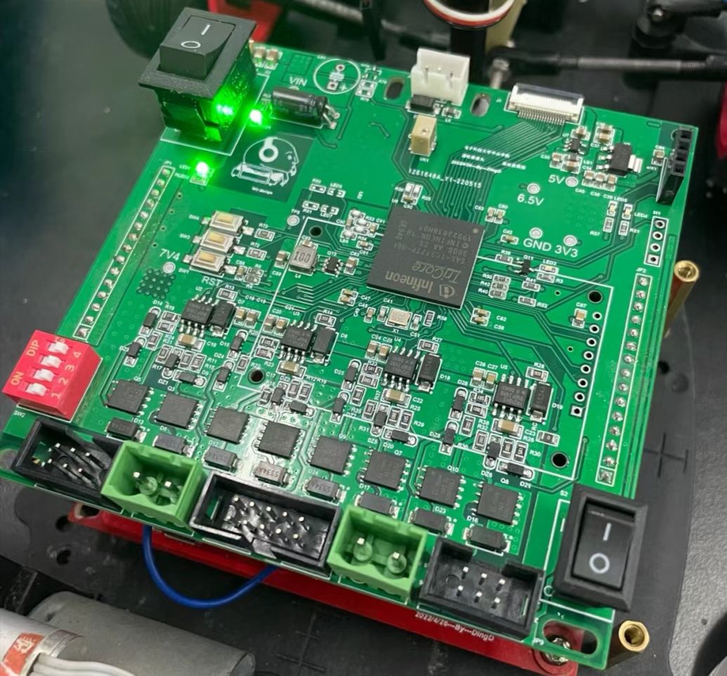
6. Pitfall: No Test Points for BGA Packages
- Common Mistake: No exposed test points for BGA pins
- Consequence: Unable to inspect soldering yield and difficult troubleshooting of post-faults
- Correct Practice: Reserve test pads around the BGA or adopt "flying probe test" compatible design
7. Pitfall: No Process Edge on Board
- Common Mistake: Mounting components directly on the PCB edge
- Consequence: Inability to fix during SMT assembly, leading to component damage
- Correct Practice: Reserve 5-8mm process edge on the board (can be trimmed later)
8. Pitfall: Silkscreen Blocking Pads
- Common Mistake: Silkscreen text/Logos covering pads
- Consequence: Solder inability to adhere, resulting in cold solder joints
- Correct Practice: Maintain a distance of ≥0.2mm between silkscreen and pads
9. Pitfall: Insufficient Spacing Between Copper Pours of Different Networks
- Common Mistake: Spacing less than 0.3mm between copper pours of different voltage networks
- Consequence: Breakdown and short circuits in high-voltage scenarios
- Correct Practice: Maintain a spacing of ≥0.5mm (enlarge according to voltage level for high-voltage boards)
10. Pitfall: Unspecified Board Thickness/Material Requirements
- Common Mistake: No indication of board thickness or material (e.g., FR4/aluminum substrate) in Gerber files
- Consequence: Manufacturer produces according to default settings, inconsistent with actual needs
- Correct Practice: Clearly specify board thickness (e.g., 1.6mm) and material type in file notes or orders; indicate substrate permittivity and other parameters for high-frequency scenarios


10585 View