
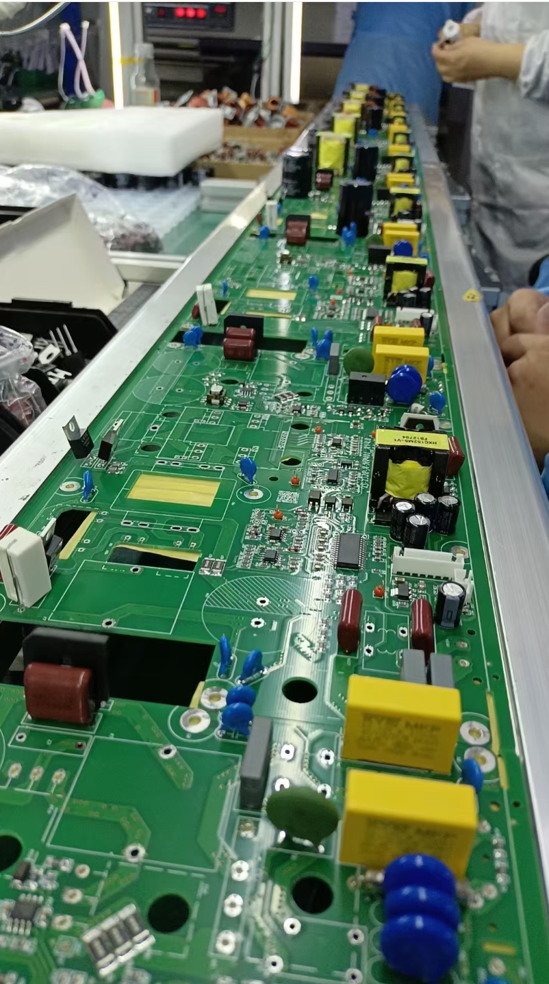
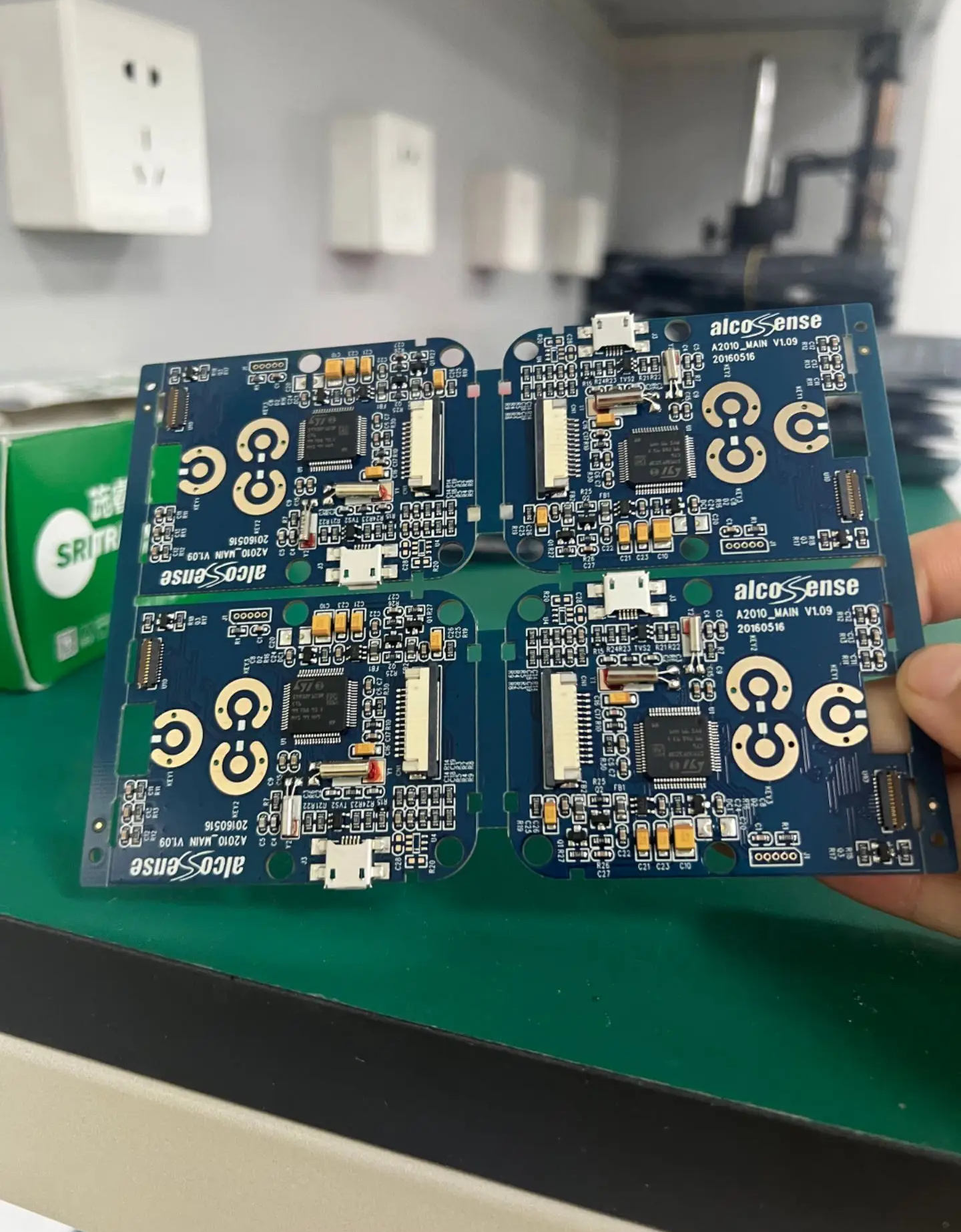
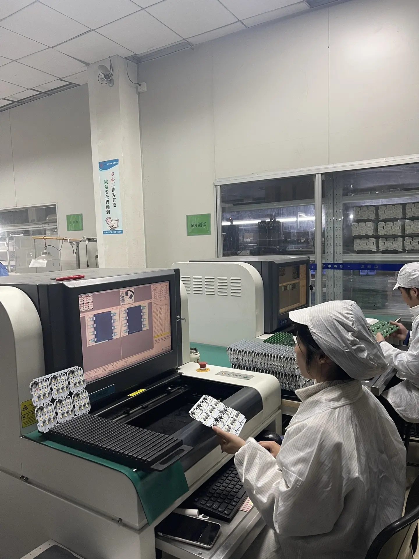
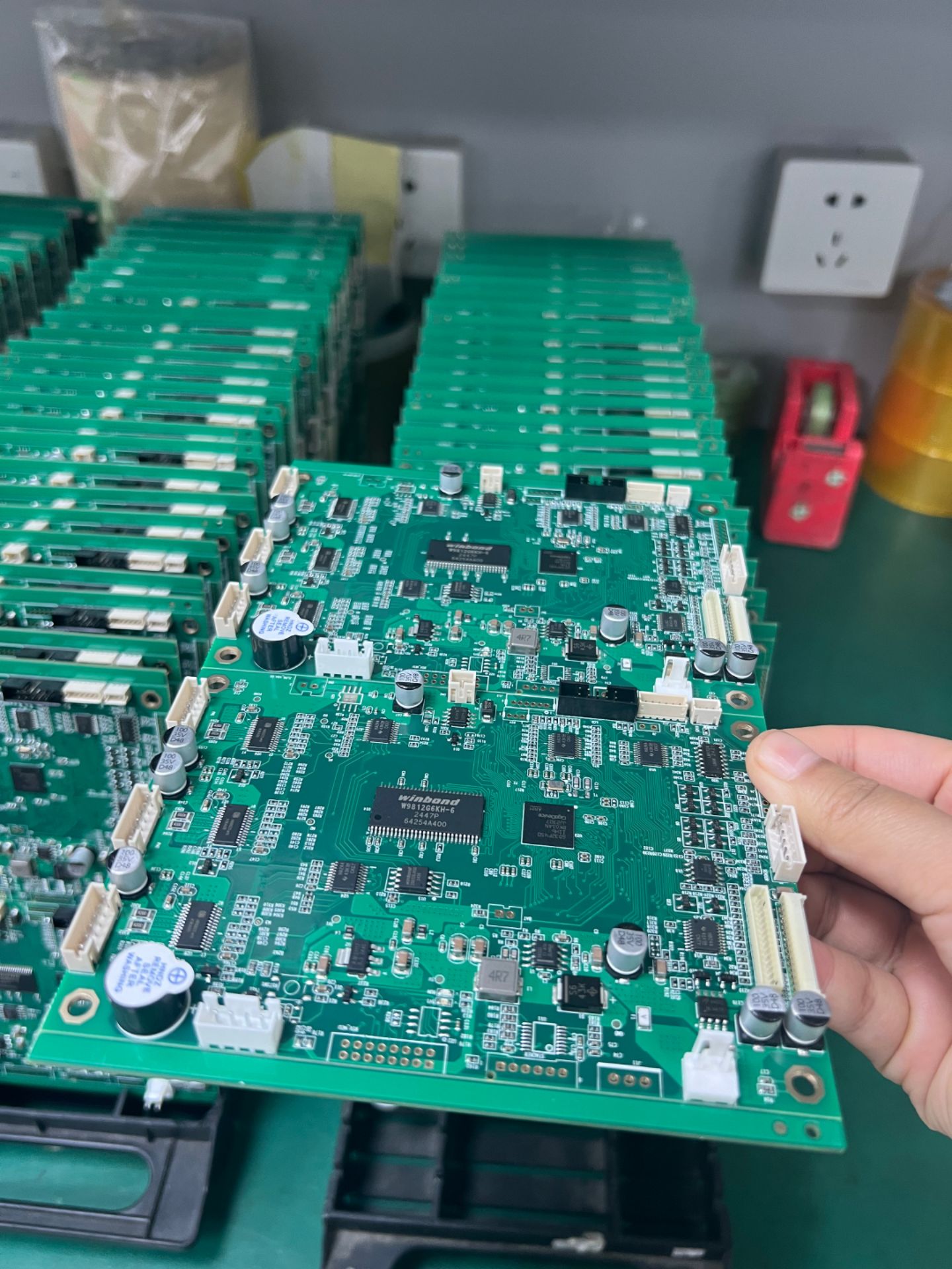
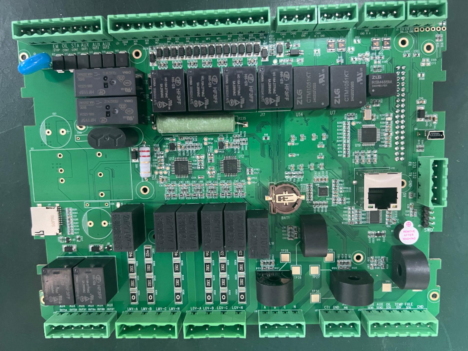
Some holes on the PCB are not through holes or blind holes. These holes are called half holes. Half holes are commonly used in HDI high-density boards. By using laser or mechanical drilling to partially打通 the copper layer and connect only to the inner or adjacent layers, higher density signal wiring can be achieved.
The main functions of half holes are threefold:
1. Save space and allow for more compact wiring.
2. Maintain signal integrity, reducing high-speed signal crosstalk and reflection.
3. Improve the reliability of the board, suitable for high-density packaging such as BGA and QFN. When designing, attention should be paid to the size and copper thickness to ensure reliable soldering and stable signals.


10585 View