
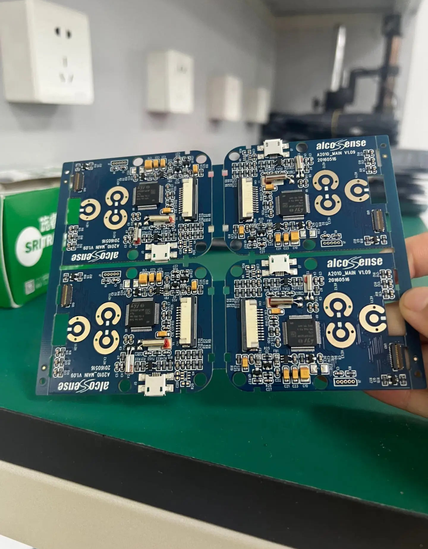
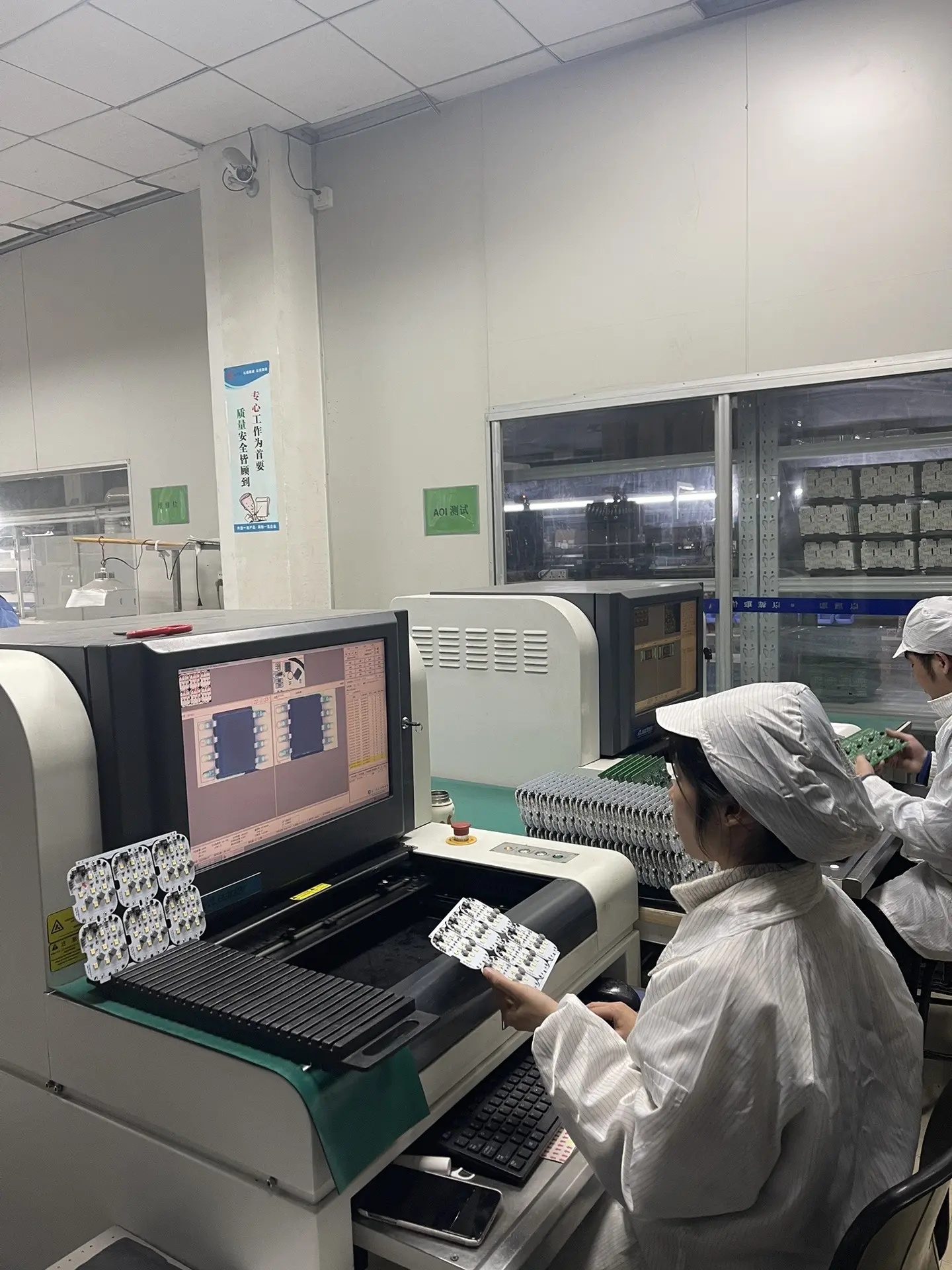
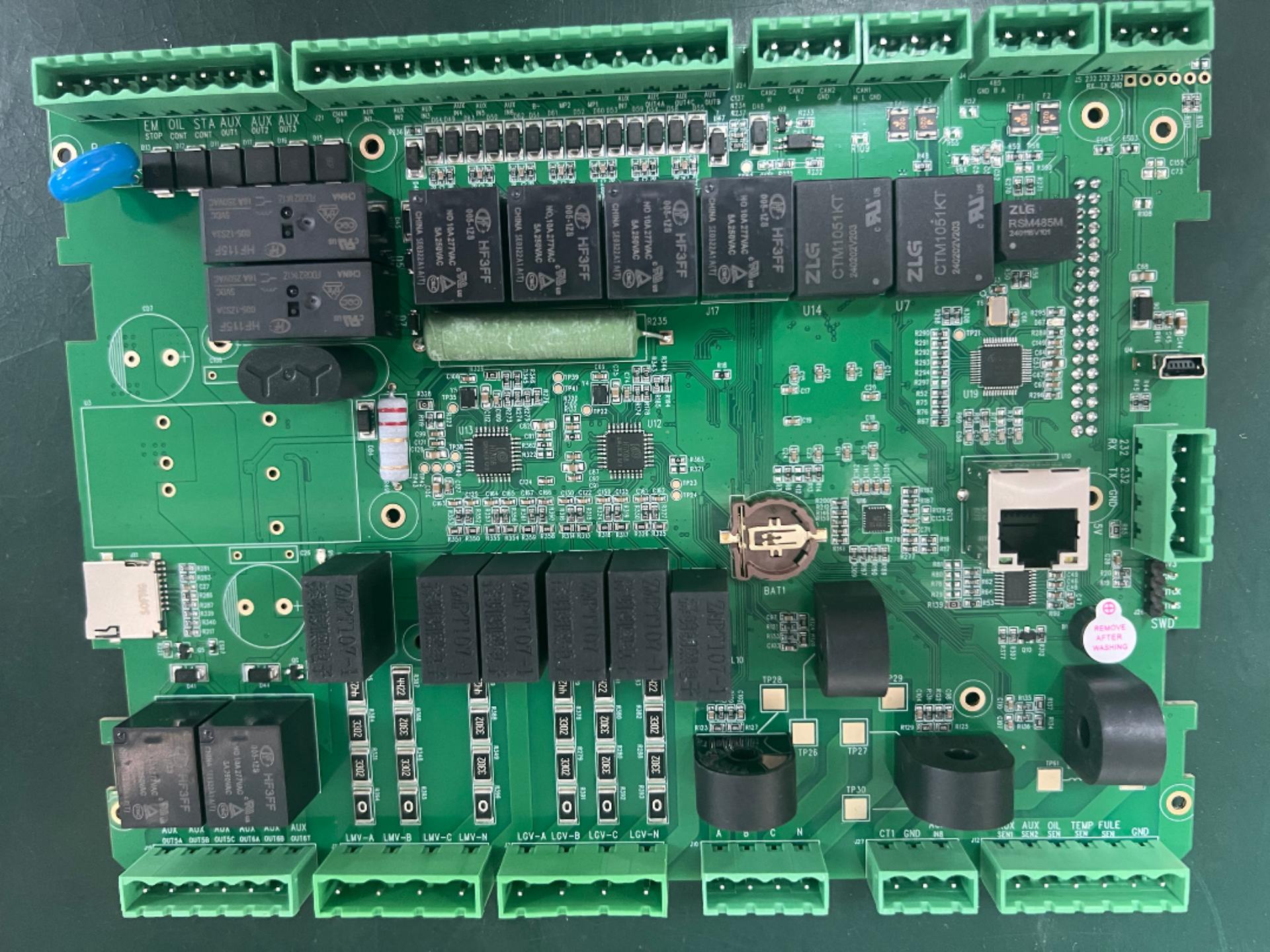
Many people see the dense small holes on a PCB but don't know they are actually called stitching vias. The function of stitching vias is to drill small holes between different layers of the PCB and connect them with copper, integrating large-area copper foils on multiple layers, such as ground layers or power layers, into a single whole.
It has six main functions:
1. Ground Connection: Reduces the impedance of return currents.
2. Interlayer Transition: Makes high-speed signal layer switching more stable.
3. Noise and EMI Control: Suppresses electromagnetic coupling.
4. Power Connection: Maintains low impedance in power paths.
5. Heat Dissipation Assistance: Guides heat to other areas.
6. Electromagnetic Shielding: Forms a via wall with guard rings to protect critical signals.
During design, note that the density of stitching vias should be determined based on frequency and EMC requirements. Avoid dense via placement too close to signal lines, and ensure sufficient connection area with ground and power layers to truly exert its effect.


10585 View