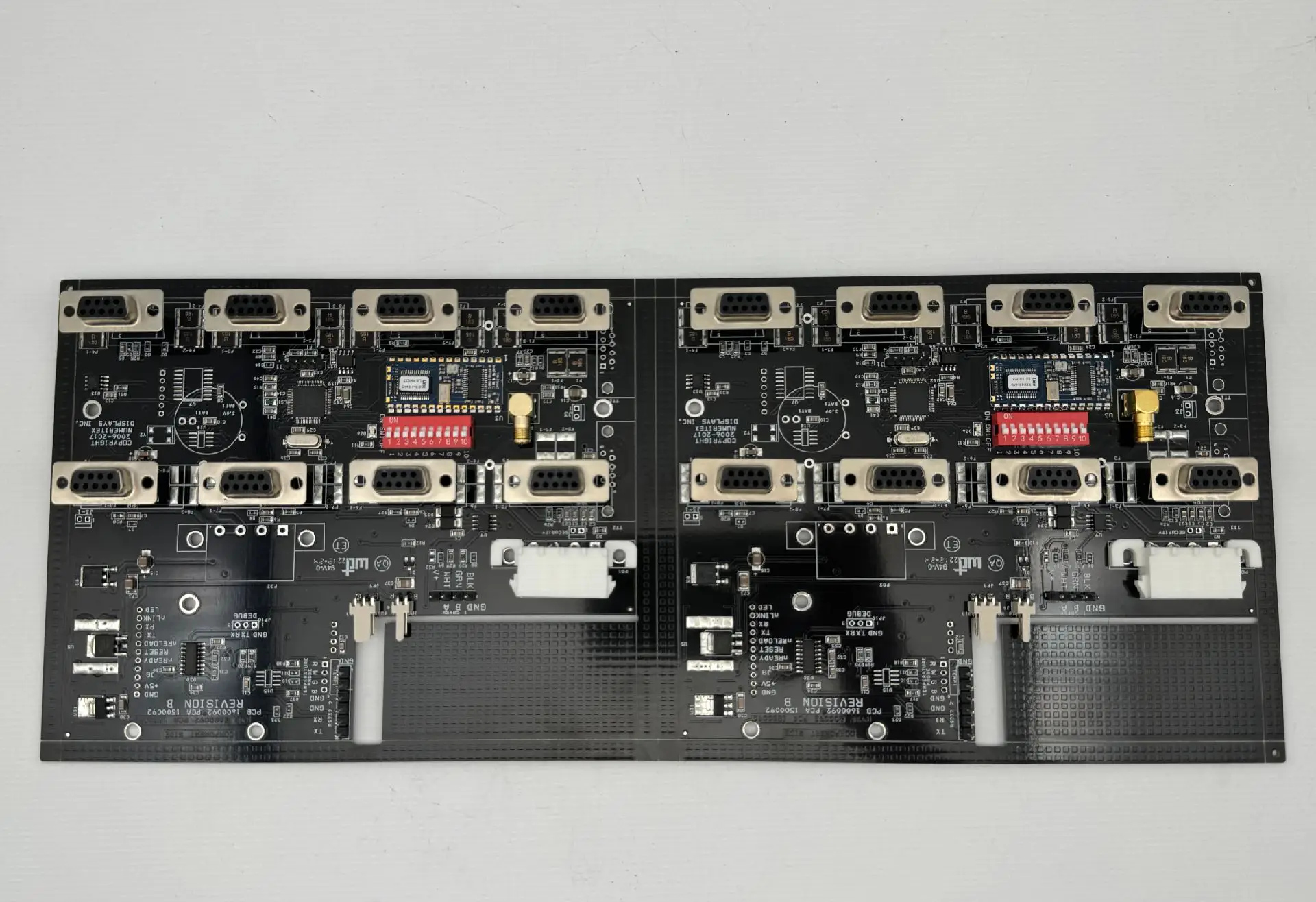
Amid the wave of electronic devices upgrading toward higher performance and miniaturization, Through Glass Via (TGV) technology has emerged as a core direction to replace traditional organic substrates and silicon interposers in the advanced packaging field, thanks to the high-frequency, low-loss and high-insulation properties of glass substrates. As the core bottleneck for its large-scale application, TGV plating is now at a critical juncture of technological breakthroughs and industrial commercialization.
What is TGV Plating?
Different from PCB Plated Through Hole (PTH) and Through Silicon Via (TSV) plating, TGV plating is a process that achieves metal conductive interconnection in micron-scale vias on glass substrates, consisting of three key steps: laser drilling → conductive seed layer deposition → electrochemical copper plating and filling. The characteristics of glass, such as non-conductivity, high brittleness and a large thermal expansion coefficient difference from metals, have led to an exponential increase in its process difficulty.
The Industrial Boom Arrives: On the Eve of Large-Scale Production
TGV technology has moved from the laboratory to the fast track of industrial layout:
✅ Robust market growth: The market size is projected to rise from $1.2 billion in 2024 to $2.5 billion in 2033, with a remarkable compound annual growth rate;
✅ Driven by high-end demand: The extreme requirements for high-speed transmission and signal integrity in AI, 5G, High-Performance Computing (HPC) and new energy vehicles have made glass substrates an ideal carrier;
✅ Accelerated industrial chain layout: Semiconductor giants including Intel and Samsung, as well as material manufacturers such as Nippon Electric Glass (NEG), have all entered R&D and trial production, targeting next-generation packaging architectures for AI chips and other products.
Core Pain Points in Mass Production: Plating Becomes the Biggest Bottleneck
The yield improvement of TGV plating is faced with multiple challenges, with the core focusing on:
🔸 High brittleness of glass substrates and stringent requirements for thickness uniformity, which are prone to microcracks and affect reliability;
🔸 Laser drilling tends to form "X-shaped" vias, and the uneven morphology of via walls increases the difficulty of plating;
🔸 Difficulties in plating solution exchange and additive diffusion in high aspect ratio vias, which are highly likely to cause internal voids, leading to increased resistance and device failure;
🔸 Process chain risks such as uneven seed layer coverage, improper temperature control in Chemical Mechanical Polishing (CMP) after plating, and thermal stress delamination at the copper-glass interface.
Technological Innovation for a Breakthrough: Empowered by New Materials and Equipment
The industry is overcoming pain points through collaborative innovation in processes, materials and equipment, with core breakthroughs including:
🔹 Disruptive process: "Dual-glass stacking + inside-out" filling, which enables copper plating to grow bidirectionally from the center of the via, stably filling vias with an aspect ratio of up to 25:1 and fundamentally avoiding void formation;
🔹 Material and parameter optimization: Multi-stage plating and precise regulation of current density improve the uniformity of plating layers; via wall pre-lubrication treatment enhances the deposition effect of the seed layer;
🔹 Upgraded special equipment: Vertical plating equipment replaces traditional horizontal plating equipment, realizing uniform distribution of metal ions in vias through eddy currents;
🔹 Full-process testing: Sub-nanoscale substrate defect detection, high-resolution X-Ray non-destructive scanning and Plasma Focused Ion Beam (PFIB) precise failure analysis build a yield assurance system.
Conclusion
TGV plating is the key bridge for glass substrates to transform from technological potential to mass production, and it is currently in a core stage of breaking through bottlenecks. With the implementation of disruptive processes such as "inside-out" plating, as well as the collaborative development of special equipment, precise control and cutting-edge testing technologies, the yield and efficiency of TGV plating are gradually moving toward the economic inflection point.
In the future, when TGV technology is applied on a large scale, glass substrates will completely reshape the interconnection pattern of advanced packaging, inject core driving force into the next generation of electronic devices such as AI and high-speed computing, and usher in a brand-new era for PCB manufacturing and semiconductor packaging.
10393 View

