Introduction: Why do "seemingly fine" boards run into trouble after assembly?
Many R&D engineers and purchasing managers face a frustrating situation: the Gerber files pass inspection, the BOM checks out perfectly, yet after SMT assembly, problems emerge—cold solder joints, unstable testing, or components that simply won't fit.
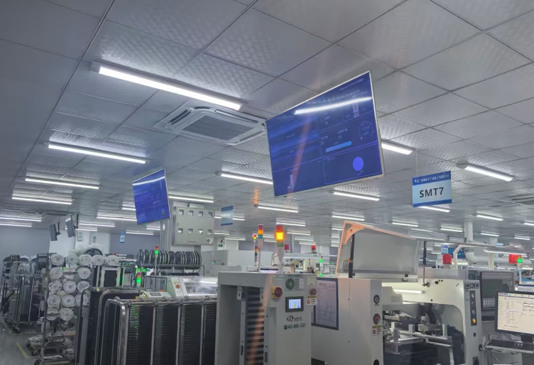
As a factory deeply engaged in PCB fabrication and PCBA assembly, we work with microscopes, reflow ovens, and wave soldering machines every day. Today, we are not discussing complex impedance calculations. Instead, we stand from the manufacturing floor perspective to talk about the small pitfalls that are invisible in design software but inevitable on the production line. This guide will help you avoid most common production issues on your next order.
---
Issue 1: "My board warps or even delaminates after reflow soldering."
(Pain Point: Board warpage, delamination, blistering)
Factory Perspective:
Many designers focus only on connectivity when designing multi-layer or heavy copper boards, neglecting stack-up symmetry and copper distribution.
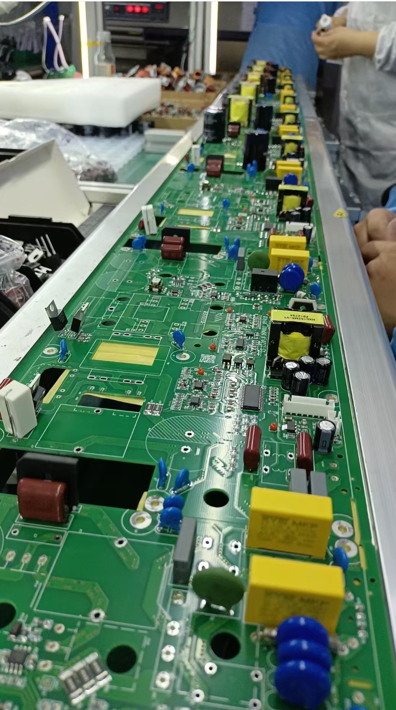
· Symptoms: During double-sided SMT, the first side reflows fine, but after the second side, the board develops a bubble in the middle (delamination) or warps like a potato chip, making it impossible to feed into the pick-and-place machine.
· Practical Advice:
1. Copper Balancing: If the top layer has a large ground pour, try to add a similar pour (hatched or solid) on the bottom layer in the corresponding area. Avoid having solid copper on one side and sparse traces on the other. Uneven thermal expansion coefficients are the primary cause of warpage and delamination.
2. Lead-Free Process Alert: If your board is thick (>2.0mm) and must endure multiple high-temperature cycles of lead-free reflow (peak ~245-250°C) followed by wave soldering, please specify "High Tg Material" when ordering. Standard mid-low Tg laminates (Tg ≤140°C) are prone to barrel cracking or inner-layer delamination under repeated thermal stress.
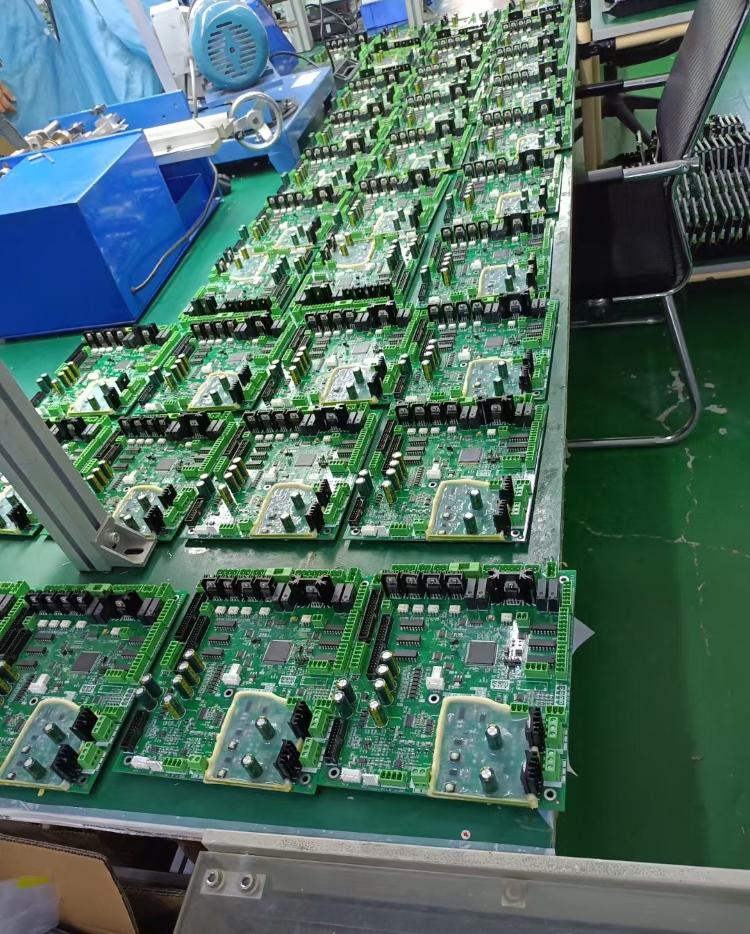
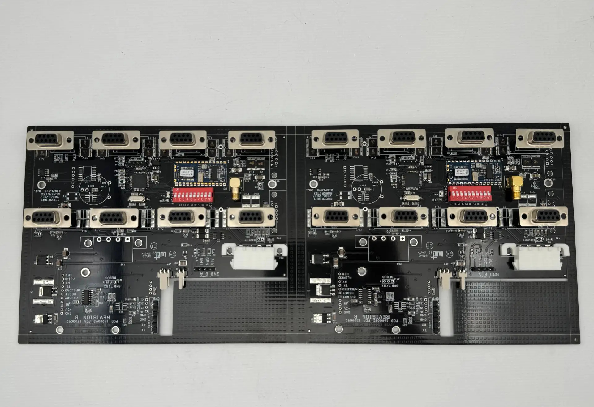
Issue 2: "The BOM is correct, but parts won't solder properly—tombstoning or cold joints?"
(Pain Point: Poor pad design, incorrect component footprint)
Factory Perspective:
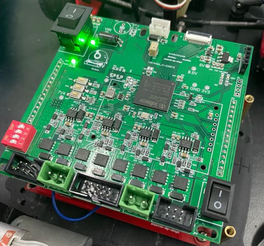
This is one of the most frequent issues in turnkey PCBA. Sometimes the purchased component is correct, but the footprint library used in the design does not match the physical part.
· Symptoms: An 0402 capacitor sitting on massive pads floats like a boat in a sea of solder (tombstoning); the center pad opening on a QFN is too large, lifting the chip and causing it to hover (open/short).
· Practical Advice:
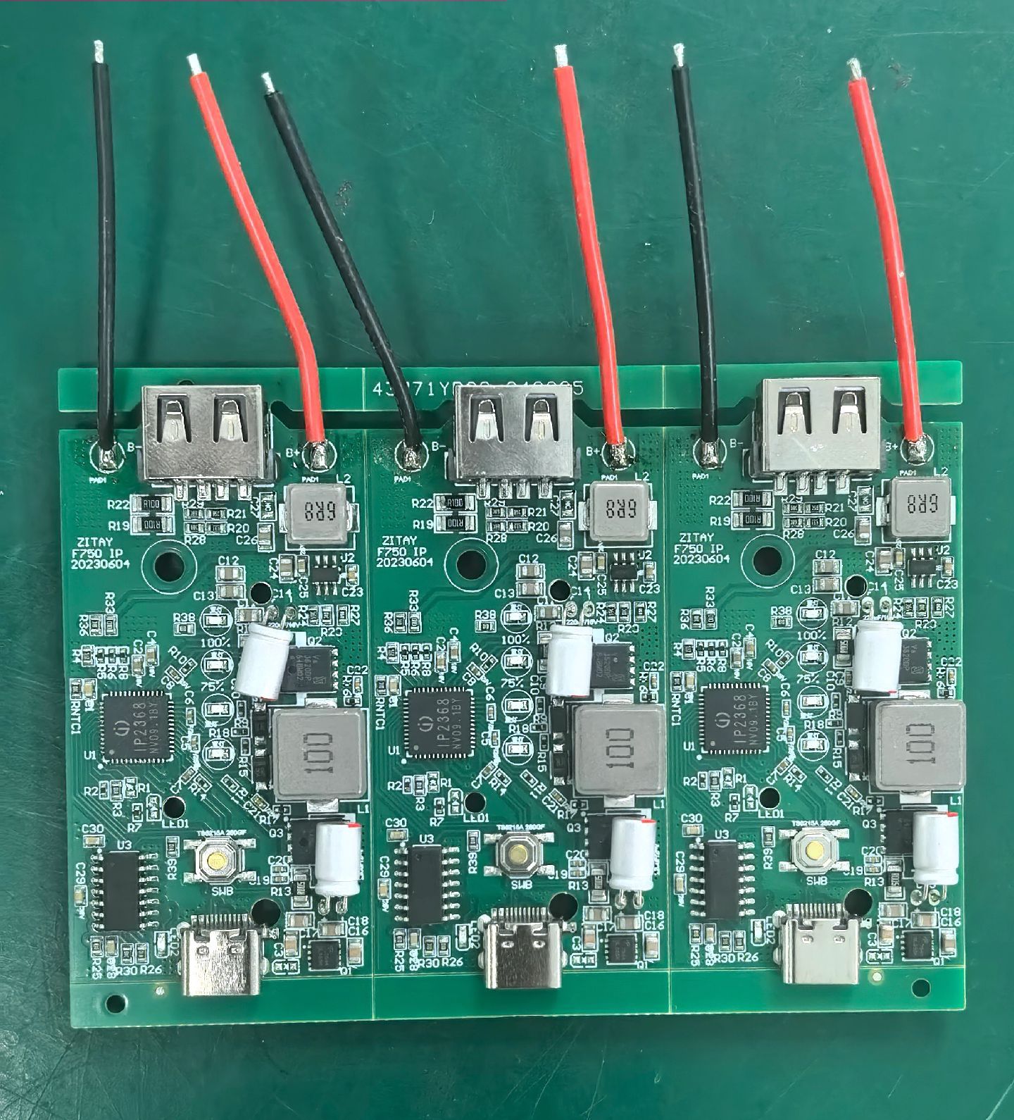
1. Physical Verification: Especially for tactile switches, USB Type-C connectors, and electrolytic capacitors. Always measure the actual part's lead spacing with calipers. Library dimensions are "nominal values." Mold tolerances across different batches of connectors can vary by up to 0.2mm—enough to prevent through-hole insertion.
2. Regarding Solder Bridging: If you experience frequent shorts on fine-pitch ICs (e.g., 0.5mm pitch and above), and the spacing allows, you can note on the order: "Keep solder mask dam between IC pins." If the gap is too narrow (<0.25mm clearance), the factory cannot maintain a dam and will advise switching to windowed openings or adjusting the design.
Issue 3: "The prototype worked perfectly. Why did the power chip burn out after building a few hundred?"
(Pain Point: Thermal design, via wicking, power integrity)
Factory Perspective:
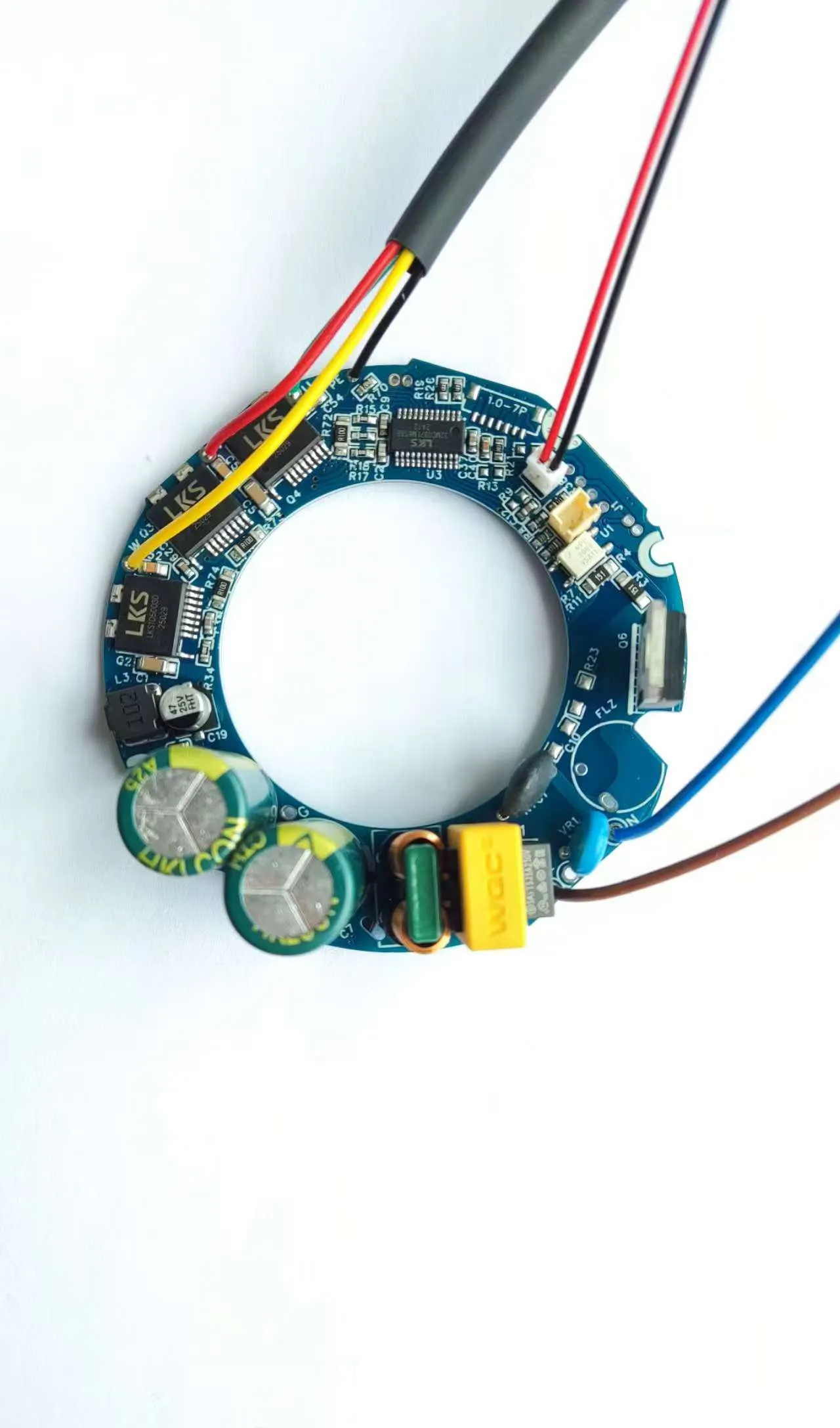
A hand-soldered prototype working does not guarantee SMT mass production success. Hand soldering creates larger thermal mass joints; reflow soldering exposes flaws in pad geometry and thermal relief.
· Symptoms: Untented thermal vias under a power inductor or MOSFET wick solder paste away during reflow, resulting in starved solder joints on the component side and unwanted solder beads/shorts on the bottom side.
· Practical Advice:
1. Thermal Via Treatment: For vias under power IC thermal pads, "Resin Plugging & Via-in-Pad Plating" is strongly recommended. If you skip this to reduce cost, ensure the solder paste stencil opening avoids those via locations to prevent paste loss.
2. Copper Weight vs. Current: If your calculated trace width for high current is borderline, consider widening the trace or requesting heavy copper (2oz or 3oz) . Running near-max current through 1oz copper over long periods often results in board yellowing and aging.
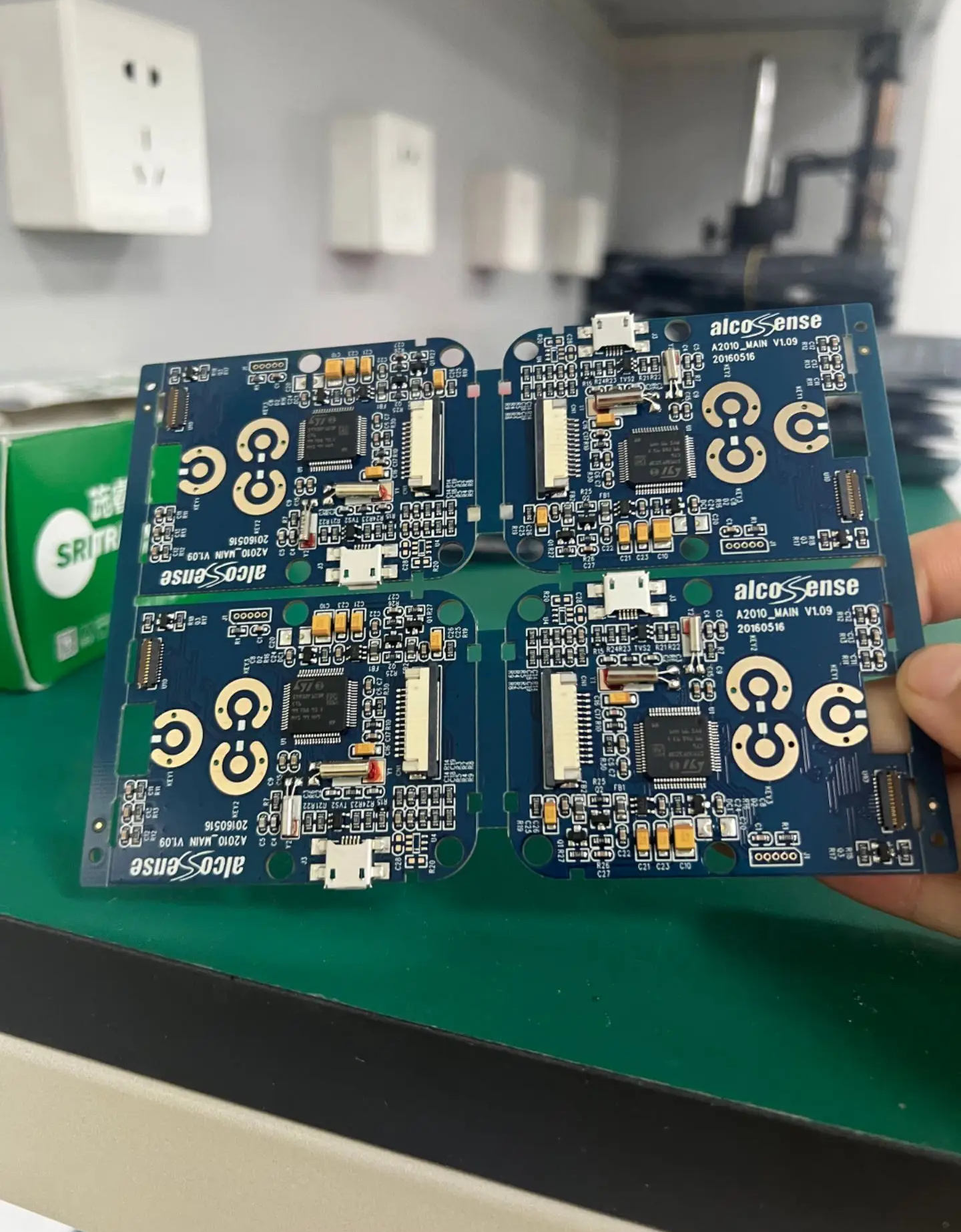
Issue 4: "Silkscreen legends are unreadable—confusing both production and repair."
(Pain Point: Overlapping silkscreen, reversed polarity, maintenance difficulty)
Factory Perspective:
Silkscreen is not just for aesthetics; it is the primary reference for pick-and-place programming and the roadmap for repair technicians.
· Symptoms: Diode/Tantalum polarity marks covered by pads; silkscreen ink printed on pads (reducing solderability); reference designators scattered inconsistently, making R38 impossible to locate.
· Practical Advice:
1. The Ultimate Solution: If board space is extremely tight, skip the white silkscreen. Draw a small arrow on the Top Layer (Copper) , then open a window on the Top Solder Mask layer over that arrow. The result is a bright gold or silver arrow that is far more durable than ink and easier for machine vision to recognize.
2. Panelization Note: When ordering panelized boards, always add fiducial marks and orientation arrows on the breakaway rails. We've seen symmetrical boards where operators could not determine feed direction, leading to components placed backwards. A small arrow on the rail significantly reduces the risk of manual inspection errors.
Issue 5: "How do I balance cost savings with maintaining quality?"
(Pain Point: Cost vs. Yield Optimization)
Factory Perspective:
We want customers to achieve the best results for the best price. There are "hidden savings" you can implement:
· Panelization & V-Scoring: Design panels as regular rectangles whenever possible to avoid irregular routing charges. If a connector hangs over the board edge, try to bring it inboard; protruding edges waste panel space and are prone to shipping damage.
· The Breakaway Rail Myth: For prototypes and small batch runs, creating a custom fixture can cost hundreds of dollars—enough to pay for adding breakaway rails to dozens of orders. Unless you are optimizing high-volume production for material savings, adding a 5mm breakaway rail is the most cost-effective choice for prototyping.
---
Conclusion:
Hardware development is demanding. Many of these "small issues" can be eliminated at the design stage with just a few minutes of communication with our engineering team.
We provide more than just PCB fabrication and PCBA assembly; we provide pre-production DFM (Design for Manufacturability) reviews.